Surface Coating Technologies
Besides manufacturing contact materials from the solid phase, i.e. by melt or powder metallurgy, the production starting in the liquid or gaseous phase is generally preferred when thin layers within the μm range are required, which cannot be obtained economically by conventional cladding methods (Table 1). Such coatings fulfill different requirements depending on their composition and thickness. They can serve as corrosion or wear protection or can fulfill the need for thin contact layers for certain technical applications. In addition they serve for decorative purposes as a pleasing and wear resistant surface coating.
| Properties | Applications | Examples |
|---|---|---|
| Color | Pleasing appearance | Brass plated lamps and furniture hardware |
| Luster | Decorative appearance, Light reflection | Chrome plated fixtures, silver coated mirrors |
| Hardness / Wear Resistance | Prolonging of mechanical wear life | Hard chrome plated tools |
| Sliding properties | Improvement of dry sliding wear | Lead-tin-copper alloys for slide bearings |
| Chemical stability | Protection against chemical effects | Lead-Tin coatings as etch resist on PC boards |
| Corrosion resistance | Protection against environmental corrosion | Zinc coatings on steel parts |
| Electrical conductivity | Surface conduction of electrical current | Conductive path on PC boards |
| Thermal conductivity | Improved heat conduction on the surface | Copper plated bottoms for cookware |
| Machining capability | Shaping through machining | Copper coatings on low pressure cylinders |
| Magnetic properties | Increase of coercive force *) | Cobalt-nickel layers on magnetic storage media |
| Brazing and soldering | Brazing without aggressive fluxes | Tin-Lead coatings on PC board paths |
| Adhesion strength | Improvement of adhesion | Brass coating on reinforcement steel wires in tires |
| Lubricating properties | Improvement of formability | Copper plating for wire drawing |
To reduce the mechanical wear of thin surface layers on sliding and connector contacts, additional lubricants in liquid form are often used. On silver contacts, passivation coatings are applied as protection against silver sulfide formation.
Contents
Coatings from the Liquid Phase
For thin coatings starting from the liquid phase, two processes are used differentiated by the metallic deposition being performed either with or without the use of an external electrical current source. The first one is electroplating, while the second one is a chemical deposition process.
Electroplating (or Galvanic Deposition)
For electroplating of metals, especially precious metals, water based solutions (electrolytes) are used, which contain the metals to be deposited as ions (i.e. dissolved metal salts). An electric field between the anode and the work pieces as the cathode, forces the positively charged metal ions to move to the cathode where they give up their charge and deposit themselves as metal on the surface of the work piece. Depending on the application, for electric and electronic or decorative end use, different electrolytic bath solutions (electrolytes) are used. The electroplating equipment used for precious metal plating and its complexity varies widely, depending on the process technologies employed. Electroplating processes are encompassing, besides the pure metal deposition, also preparative and post treatments of the goods to be coated. An important parameter for creating strongly adhering deposits is that the surface of the goods has to be metallic clean without oily or oxide film residues. This is achieved through various pre-treatment processes, specifically developed for the types of material and surface conditions of the goods to be plated. In the following segments, electrolytes – both precious and non-precious – as well as the most widely used electroplating processes are described.
Main Articel: Electroplating (or Galvanic Deposition)
Electroless Plating
Electroless plating is defined as a coating process which is performed without the use of an external current source. It allows a uniform metal coating, independent of the geometrical shape of the parts, to be coated. Because of the very good dispersion capability of the used electrolytes, also cavities and the inside of drilled holes in parts can be coated for example. In principal, two different mechanisms are employed for electroless plating: processes in which the carrier material serves as a reduction agent (Immersion processes) and those in which a reduction agent is added to the electrolyte (Electroless processes).
Main Articel: Electroless Plating
Coatings from the Gaseous Phase (Vacuum Deposition)
The term PVD (physical vapor deposition) defines processes of metal, metal alloys and chemical compounds deposition in a vacuum by adding thermal and kinetic energy by particle bombardment. The main processes are the following four coating variations (Table 2):
- Vapor deposition
- Sputtering (Cathode atomization)
- Arc vaporizing
- Ion implantation
In all four processes, the coating material is transported in its atomic form to the substrate and deposited on it as a thin layer (a few nm to approx. 10 μm)
| Process | Principle | Process Gas Pressure | Particle Energy | Remarks |
|---|---|---|---|---|
| Vapor deposition | Vaporizing in a crucible (electron beam or resistance heating) |
10-3 Pa | < 2eV | Separation of alloy components may occur |
| Arc vaporizing | Vaporizing of the target plate in an electrical arc |
10-1 Pa-1Pa | 80eV-300eV | Very good adhesion due to ion bombardement |
| Sputtering | Atomizing of the target plate (cathode) in a gas discharge |
10-1 Pa-1Pa | 10eV-100eV | Sputtering of non-conductive materials possible through RF operation |
| Ion implantation | Combination of vapor deposition and sputtering |
10-1 Pa-1Pa | 80eV-300eV | Very good adhesion from ion bombardment but also heating of the substrate material |
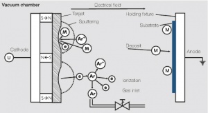
The sputtering process has gained the economically most significant usage. Its process principle is illustrated in (Figure 1).
Initially, a gas discharge is ignited in a low pressure (10-1 -1 Pa) argon atmosphere. The argon ions generated, are accelerated in an electric field and impact the target of material to be deposited with high energy. Caused by this energy, atoms are released from the target material which condensate on the oppositely arranged anode (the substrate) and form a layer with high adhesion strength. Through an overlapping magnetic field at the target location, the deposition rate can be increased, making the process more economical.
The advantages of the PVD processes and especially sputtering for electrical contact applications are:
- High purity of the deposit layers
- Low thermal impact on the substrate
- Almost unlimited coating materials
- Low coating thickness tolerance
- Excellent adhesion (also by using additional intermediate layers)
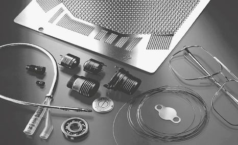
Coatings produced by PVD processes are used for contact applications, for example on miniature-profiles, in electrical engineering and for electronic components, for solderability in joining processes, for metalizing of nonconductive materials, as well as in semiconductors, opto-electronics, optics and medical technology applications.
There are few limitations regarding the geometrical shape of substrate parts. Only the interior coating of drilled holes and small diameter tubing can be more problematic (ratio of depth to diameter should be < 2:1). Profile wires, strips and foils can be coated from one side or both; formed parts can be coated selectively by using masking fixtures that at the same time serve as holding fixtures (Figure 2).
- Materials
Selection of possible combinations of coating and substrate materials
Substrate Materials | Coating Materials | |||||||||||
|---|---|---|---|---|---|---|---|---|---|---|---|---|
Ag | Au | Pt | Pd | Cu | Ni | Ti | Cr | Mo | W | Ai | Si | |
Precious metal / alloys | ||||||||||||
NF metals / alloys | ||||||||||||
Fe alloys / stainless steel | ||||||||||||
Special metals (Ti, Mo, W) | ||||||||||||
Carbide steels (WC-Co) | ||||||||||||
Ceramics (Al2O3, AlN) | ||||||||||||
Glasses (SiO2, CaF) | ||||||||||||
Plastics (PA, PPS) | ||||||||||||
![]() can be produced
can be produced
![]() can be produced with intermediate layer
can be produced with intermediate layer
- Dimensions
| Dimensions | |
|---|---|
| Coating thickness: | 10 nm - 15 μm |
| Coating thicknesses for contact applications: | 0.1 - 10 μm |
For the geometry of semi-finished products to be coated, there are few restrictions. Only the coating of the inside of machined holes and tubing has limitations.
- Tolerances
Coating thickness ±10 - 30 %, depending on the thickness
- Quality criteria
Depending on the application, the following parameters are tested and recorded (see also: Electroplating of parts):
- Coating thickness
- Solderability
- Adhesion strength
- Bonding property
- Porosity
- Contact resistance
These quality tests are performed according to industry standards, internal standards and customer specifications resp.
Comparison of Deposition Processes
The individual deposition processes have in part different performance characteristics. For each end application, the optimal process has to be chosen, considering all technical and economical factors. The main selection criteria should be based on the electrical and mechanical requirements for the contact layer and on the design characteristics of the contact component. Table 3 gives some indications for a comparative evaluation of the different coating processes.
The electroless metal coating is not covered here because of the low thickness of deposits, which makes them in most cases not suitable for contact applications.
| Process / Coating Properties | Mechanical Processes (Cladding) | Electroplating | Vaccum Deposition (Sputtering) |
|---|---|---|---|
| Coating material | formabe metal and alloys | metals, alloys only limited | metals and alloys |
| Coating thickness | > 1μm | 0.1 - approx. 10 μm (in special cases up to 100 μm) |
0.1 approx. 10 μm |
| Coating configuration | selectively, stamping edges not coated | all around and selectively stamping edges coated |
mostly selectivity |
| Adhesion | good | good | very good |
| Ductility | good | limited | good |
| Purity | good | inclusions of foreign materials | very good |
| Porosity | good | good for > approx. 1μm | good |
| Temperature stability | goodvery good | good | very good |
| Mechanical wear | little | very little | little |
| Environmental impact | little | significant | none |
The main differences between the coating processes are found in the coating materials and thickness. While mechanical cladding and sputtering allow the use of almost any alloy material, electroplating processes are limited to metals and selected alloys, such as for example high-carat gold alloys with up to .3 wt% Co or Ni. Electroplated and sputtered surface layers have a technological and economical upper thickness limit of about 10μm. While mechanical cladding has a minimum thickness of approx. 1 μm, electroplating and sputtering can also be easily applied in very thin layers down to the range of 0.1 μm.
The properties of the coatings are closely related to the coating process. Starting materials for cladding and sputtering targets precious metals and their alloys, which in the case of gold and palladium based materials, are vacuum melted and therefore exhibit a very high purity. During electroplating, depending on the type of electrolytes and the deposition parameters, some electrolyte components such as carbon and organic compounds are incorporated into the precious metal coating. Layers deposited from the gaseous phase however are very pure.
Hot (-Dipped) Tin Coated Strip Materials
During hot-dip tinning, pre-treated strip materials are coated with pure tin or tin alloys from a liquid solder metal. During overall (or all-around) tinning the strips through a liquid metal melt. For strip tinning, rotating rolls are partially immersed into a liquid tin melt and transport the liquid onto the strip, which is guided above them. Through special wiping and gas blowing procedures, the deposited tin layer can be held within tight tolerances. Hot tinning is performed directly onto the base substrate material without any pre-coating with either copper or nickel. Special cast-on processes or the melting of solder foils onto the carrier strip, also allows the production of thicker solder layers ( > 15 μm).
The main advantage of hot tinning of copper and copper alloys, compared to tin electroplating, is the formation of an inter-metallic copper-tin phase (Cu3Sn, Cu6Sn5) at the boundary between the carrier material and the tin layer. This thin (0.3 – 0.5 μm) intermediate layer, which is formed during the thermal tinning process, is rather hard and reduces the frictional force and mechanical wear in connectors. Tin coatings produced by hot tinning have a good adhesion to the substrate material and do not tend to tin whisker formation.
A special process of hot tinning is the “Reflow” process. After depositing a tin coating by electroplating, the layer is short-time melted in a continuous process. The properties of these reflow tin coatings are comparable to those created by conventional hot tinning.
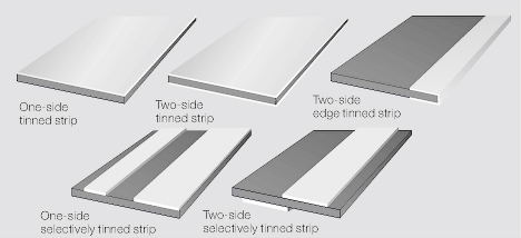
Besides overall tin coating of strip material, the hot tinning can also be applied in the form of single or multiple stripes on both sides of a continuous substrate strip (Figure 3).
- Materials
Coating materials: Pure tin, tin alloys
Substrate materials: Cu, CuZn, CuNiZn, CuSn, CuBe and others
- Dimensions and Tolerances
| Width of tinning: | ≥ 3 ± 1 mm |
| Thickness of tinning: | 1 - 15 μm |
| Tolerances (thickness): | ± 1 - ± 3 μm depending on tin thickness |
- Quality Criteria
Mechanical strength and dimensional tolerances of hot tinned strips are closely related to the standard for Cu and Cu alloy strips according to DIN EN 1652 and DIN EN 1654. Quality criteria for the actual tin coatings are usually agreed upon separately.
Contact Lubricants
By using suitable lubricants, the mechanical wear and frictional oxidation of sliding and connector contacts can be substantially reduced. In the electrical contact technology, solid as well as high and low viscosity liquid lubricants are used.
Contact lubricants have to fulfill a multitude of technical requirements:
- They must wet the contact surface well; after the sliding operation the lubrication film must close itself again, i.e. mechanical interruptions to heal
- They should not transform into resins, not evaporate, and not act as dust collectors
- The lubricants should not dissolve plastics, they should not be corrosive to non-precious metals or initiate cracking through stress corrosion of plastic components
- The specific electrical resistance of the lubricants cannot be so low that wetted plastic surfaces lose their isolating properties
- The lubricant layer should not increase the contact resistance; the wear reducing properties of the lubricant film should keep the contact resistance low and consistent over the longest possible operation time
Solid lubricants include for example 0.05 – 0.2 μm thin hard gold layers, which are added as surface layers on top of the actual contact material.
Among the various contact lubricants offered on the market, contact lubrication oils have shown performance advantages. They are mostly synthetic, chemically inert and silicone-free oils which differ in their chemical composition and viscosity.
For sliding contact systems with contact forces < 50 cN and higher sliding speeds, oils with a lower viscosity (< 50 mPa·s) are preferential. For applications with higher contact forces and operating at higher temperatures, contact oils with a higher viscosity are advantageous. Contact oils are mainly suited for applications at low current loads. At higher loads and in situations where contact separation occurs during the sliding operation, thermal decomposition may be initiated, which causes the lubricating properties to be lost.
Passivation of Silver Surfaces
The formation of silver sulfide during the shelf life of components with silver surface in sulfur containing environments, can be significantly eliminated by coating them with an additional protective film layer (Passivation layer). For electrical contact use, such thin layers should be chemically inert and sufficiently conductive, otherwise they are easily broken by the applied contact force.
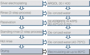
The passivation process SILVERBRITE W ATPS is a water-based tarnish preventer for silver (Figure 4). It is free of chromium(VI) compounds and solvents. The passivating layer is applied by immersion, which creates a transparent organic protective film which barely changes the appearance and only slightly increases the good electrical properties such as for example the contact resistance. The good solderability and bond properties of silver are not negatively affected. Because of its chemical composition, this protective layer has some lubricating properties which reduce the insertion and withdrawal forces of connectors noticeably.
References
Vinaricky, E. (Hrsg.): Elektrische Kontakte, Werkstoffe und Anwendungen. Springer-Verlag, Heidelberg 2002
Ganz, J.; Heber, J.; Macht, W.; Marka, E.: Galvanisch erzeugte Edelmetallschichten für elektrische Kontakte. Metall 61 (2007) H.6, 394-398
Song, J.: Edelmetalle in Steckverbindungen - Funktionen und Einsparpotential. VDE - Fachbericht 67 (2011) 13-22
Heber, J.: Galvanisch abgeschiedene Rhodiumschichten für den dekorativen Bereich. Galvanotechnik, 98 (2007) H.12, 2931-2935
Johler, W.; Pöffel, K.; Weik, G.; Westphal, W.: High Temperature Resistance th Galvanically Deposited Gold Layers for Switching Contacts. Proc. 15 Holm Conf. on Electrical Contacts, Chicago (2005) 48-54
Grossmann, H. Schaudt, G.: Untersuchung über die Verwendbarkeit von Überzügen der Platinmetallgruppe auf elektrotechnischen Verbindungselementen. Galvanotechnik 67 (1976) 292-297
Grossmann, H.; Vinaricky, E.: Edelmetalleinsparung in der Elektrotechnik durch selektives Galvanisieren. In: Handbuch der Galvanotechnik. München, Hanser- Verlag, 37 (1981) 132-141
Grossmann, H.; Schaudt, G.: Hochgeschwindigkeitsabscheidung von Edelmetallen auf Kontaktwerkstoffen. Galvanotechnik 84 (1993) H.5, 1541-1547
Bocking, C.; Cameron, B.: The Use of High Speed Selective Jet Electrodeposition of Gold for the Plating of Connectors. Trans. IMF. 72 (1994) 33-40
Endres, B.: Selektive Beschichtungen von Kontaktmaterial im Durchzugsverfahren. Metalloberfläche 39 (1985) H.11, 400-404
Kaspar, F.; Marka, E.; Normann, N.: Eigenschaften von chemisch Nickel Goldschichten für Baugruppen der Elektrotechnik. VDE Fachbericht 47 (1995) 19-27
Schmitt; W.; Kißling, S.; Behrens, V.: Elektrochemisch hergestellte Schichtsysteme auf Aluminium für Kontaktanwendungen. VDE - Fachbericht 67 (2011) 136-141
Freller, H.: Moderne PVD-Technologien zum Aufbringen dünner Kontaktschichten. VDE-Fachbericht 40 (1989) 33-39
Ganz, J.: PVD-Verfahren als Ergänzung der Galvanik. Metalloberfläche 45 (1991)
Schmitt, W.; Franz, S.; Heber, J.; Lutz, O.; Behrens, V.: Formation of Silver Sulfide Layers and their Influence on the Electrical Characteristics of Contacts in th the Field of Information Technology. Proc. 24 Int. Conf.on Electr. Contacts, Saint Malo, France (2008) 489-494
Buresch, I; Ganz, J.; Kaspar, F.: PVD-Beschichtungen und ihre Anwendungen für Steckverbinder. VDE-Fachbericht 59 (2003) 73-80
Gehlert, B.: Edelmetalllegierungen für elektrische Kontakte. Metall 61 (2007) H.6, 374-379
Ganz, J.: Einsatz von Sputterverfahren bei komplexen Beschichtungsaufgaben. JOT 11 (1997)
Buresch, I.; Bögel, A.; Dürrschnabel, W.: Tin Coating for Electrical Components. Metall 48 (1994) H.1, 11-14
Buresch, I.; Horn, J.: Bleifreie Zinnoberflächen. VDE-Fachbericht 61 (2005) 89-94
Adler, U.; Buresch, I.; Riepe, U.; Tietz, V.: Charakteristische Eigenschaften der schmelzflüssigen Verzinnung von Kupferwerkstoffen. VDE-Fachbericht 63 (2007) 175-180
Huck, M.: Einsatz von Schmiermitteln auf Gleit- und Steckkontakten. Metalloberfläche (1982) 429-435
Abbott, W.,H.: Field and Laboratory Studies of Corrosion Inhibiting Lubricants for Gold-Plated Connectors. Proc. HOLM Conf.on Electrical Contacts, Chicago (1996) 414-428
Noel, S.; Alarmaguy, D.; Correia, S.; Gendre, P.: Study of Thin Underlayers to Hinder Contact resistance Increase Due to Intermetallic Compound Formation. th Proc. 55 IEEE Holm Conf. on Electrical Contacts, Vancouver, BC, Canada (2009) 153 – 159
Weik, G.; Johler, W.; Schrank, C.: Zuverlässigkeit und Eigenschaften von Gold – Schichten bei hohen Einsatztemperaturen. VDE – Fachbericht 65, (2009) 13 – 21
Buresch, I.; Hack, M.: Eigenschaften von Zinnschichten für elektromechanische Bauelemente – Einflussfaktoren und ihre Auswirkungen. VDE – Fachbericht 65, (2009) 23 – 30
Buresch, I.: Effekte intermetallischer Phasen auf die Eigenschaften von Zinnoberflächen auf Kupferlegierungen. VDE – Fachbericht 67 (2011) 38-46
Schmitt, W.; Heber, J.; Lutz, O.; Behrens, V.: Einfluss des Herstellverfahrens auf das Korrosions- und Kontaktverhalten von Ag – Beschichtungen in schwefelhaltiger Umgebung. VDE – Fachbericht 65 (2009) 51 – 58


