Difference between revisions of "Electroless Plating"
Doduco Admin (talk | contribs) (→Electroless Deposition of Nickel/Gold) |
Doduco Admin (talk | contribs) (→Immersion Deposition of Tin) |
||
| Line 63: | Line 63: | ||
<figure id="fig:Process flow for electroless tin deposition using the DODUSTAN process"> | <figure id="fig:Process flow for electroless tin deposition using the DODUSTAN process"> | ||
| − | [[File:Process flow for electroless tin deposition using the DODUSTAN process.jpg|right|thumb|Process flow for electroless tin deposition using the DODUSTAN process]] | + | [[File:Process flow for electroless tin deposition using the DODUSTAN process.jpg|right|thumb|Figure 3: Process flow for electroless tin deposition using the DODUSTAN process]] |
</figure> | </figure> | ||
Revision as of 13:31, 3 January 2023
Contents
Electroless Plating
Electroless plating is defined as a coating process which is performed without the use of an external current source. It allows a uniform metal coating independent of the geometrical shape of the parts to be coated. Because of the very good dispersion capability of the used electrolytes, also cavities and the inside of drilled holes in parts can be coated for example. In principal, two different mechanisms are employed for electroless plating: processes in which the carrier material serves as a reduction agent (Immersion processes) and those in which a reduction agent is added to the electrolyte (Electroless processes).
Immersion Processes
The immersion processes are usually applied in the plating of the metals gold, silver and tin. If the material to be coated is less precious, i.e. exhibits a negative standard potential against the metal ions in the surrounding solution, it goes into solution releasing electrons while the more precious metal ions are reduced by absorbing electrons and being deposited on the electrode. This process can continue until the complete surface of the substrate is covered with a thin layer of the more precious metal. This limits the maximum achievable layer thickness to approx. 0.1 μm. Table 1.
| Type of Electrolyte | pH-Range | Coating Properties | Application Ranges | |
|---|---|---|---|---|
| Hardness HV 0.025 | Punity | |||
| Immersion Gold electrolytes | ||||
| AUROL 4 AUROL 16 AUROL 20 |
3.8 - 4.2 5.8 - 6.2 5.8 - 6.2 5.8 - 6.2 |
60 - 80 60 - 80 60 - 80 60 - 80 |
99.99% Au 99.99% Au 99.99% Au 99.99% Au |
Thin gold layers on Ni, Ni alloys, Fe and Fe alloys for PCB technology and technical applications |
Electroless Processes
The electroless metal plating with the addition of reduction agents to the electrolyte, is based on the oxidation of the reducing agent with release of electrons, which then in return, reduce the metal ions. To achieve a controlled deposition from such solutions, the metal deposition must happen through the catalytic influence of the substrate surface.
Otherwise a "wild" uncontrollable deposition would occur. In most cases, palladium containing solutions are used for the activation, which seed the surfaces with palladium and act as catalyst in the copper and nickel electrolytes.
The electrolytes contain, besides the complex ion compounds of the metals to be deposited, also stabilizers, buffer and accelerator chemicals and a suitable reduction agent.
These electrolytes are usually operating at elevated temperatures (50° – 90°C). The deposits contain - besides the metals - also process related foreign inclusions such as for example decomposition products of the reduction agents. The electroless processes are used mainly for copper, nickel and gold deposits.
Electroless Deposition of Nickel/Gold
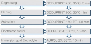
Electroless deposited nickel coatings with an additional immersion layer of gold gaining increased importance in the coating of printed circuit boards (PCBs). The process sequence is shown in Figure 1 using the example of the DODUCHEM process.
After the pre-cleaning (degreasing and etching) a palladium sulfate activator is used, which activates the exposed copper surfaces on the printed circuit board and thus facilitates the nickel deposition. The electroless working chemical nickel electrolyte contains – besides other ingredients – Sodium-hypophosphite, which is reduced to phosphorus in a parallel occurring process and incorporated into the nickel deposit. At the temperature of 87 – 89°C a very homogeneous nickel-phosphorus alloy layer with approx. 9 wt% P is deposited with layer thicknesses > 5 μm possible. During a consecutive processing step, a very thin and uniform layer (< 0.1 μm) of gold is added in an immersion electrolyte. This protects the electroless nickel layer against corrosion, achieving a solderable and well bondable surface for thick or fine aluminum bond wires.
It is possible to enhance this layer combination further by adding an immersive palladium layer between the electroless nickel and the gold coating (DODUBOND process). This Pd layer acts as a diffusion barrier and allows the usage of this surface combination also for gold wire bonding.
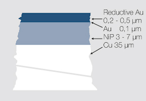
As an alternative for gold wire bonding applications, a thicker gold layer of 0.2 – 0.5 μm can be applied using an electroless process. Typical electrolytes work at a temperature of approx. 80°C with deposition rates of 0.3 – 0.4 μm per 30 minutes. There are however limitations with these electroless electrolytes concerning their stability and the robustness of the process, compared to other electroplating processes which reduces their wider usage (Figure 2).
Immersion Deposition of Tin
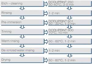
A tin coating by ion exchange is usually not possible, since copper is the more precious metal. By adding thio-urea the electro-chemical potential of copper is reduced to a level (approx. 450 mV, significantly lower than tin) that allows the exchange reaction. Using a suitable electrolyte composition and enhancer solutions like within the DODUSTAN process (Figure 3) The tin coatings produced in that way, even under usually unfavorable conditions of copper concentrations of 7 g/l in the electrolyte, are well solderable.
The immersion tin deposition is suitable for the production of a well solderable surface on printed circuit boards and electronic components. It is also used as an etch resist against ammonia based solutions or as corrosion and oxidation protection of copper surfaces.


