Switching Contacts

From Electrical Contacts
Jump to: navigation, search

Switching Contacts

    Effects during switching operations
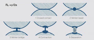
    Figure 1: Contact opening with arc formation (schematic)

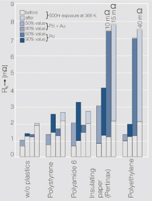
    Influence of out-gasing from plastics

    Figure 2: Histogram of the contact resistance RK of an electroplated palladium layer (3 μm) with and without hard gold flash plating (0.2 μm) after exposure with different plastic materials
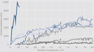
    Figure 3: Contact resistance with exposure to out-gasing from plastics as a function of numbers of operations at 6 VDC,100 mA: 1 Silicon containing plastic; 2 Plastics with strongly out-gasing components; 3 Plastics with minimal out-gasing components


    Influence of corrosive gases on the contact resistance
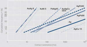

    Figure 4: Distribution of cumulative frequency H of the contact resistance for solid contact rivets after 10 days exposure in a three-component test environment with 400 ppb each of H2S, SO2 and NO2 at 25°C, 75% RH; Contact force 10cN; Measuring parameters: ≤ 40 mVDC,10 mA; Probing contact: Gold rivet
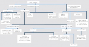
    Figure 5: Influences on contact areas in relays


    Contact Phenomena under the influence of arcing Matertia

      Material transfer
      Figure 6: Material transfer under DC load a) Cathode; b) Anode.
      Material: AgNi0.15; Switching parameters: 12VDC, 3 A, 2x10⁶ perations

      Arc erosion

      Figure 7: Arc erosion of a Ag/SnO2 contact pair after extreme arcing conditions a) Overall view; b) Partial detail view

      Contact welding

      Figure 8: Micro structure of a welded contact pair (Ag/SnO288/12 - Ag/CdO88/12) after extremely high current load. a) Ag/SnO288/12; b) Ag/CdO88/12

References

References