Difference between revisions of "Switching Contacts"
From Electrical Contacts
Doduco Admin (talk | contribs) |
Doduco Admin (talk | contribs) |
||
| Line 32: | Line 32: | ||
contact: Gold rivet</caption>]] | contact: Gold rivet</caption>]] | ||
</figure> | </figure> | ||
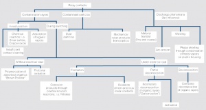
| + | [[File:Influences on contact areas in relays.jpg|right|thumb|Influences on contact areas in relays]] | ||
</div> | </div> | ||
<div class="clear"></div> | <div class="clear"></div> | ||
| − | |||
| − | |||
<li>'''Contact Phenomena under the influence of arcing Matertia'''</li> | <li>'''Contact Phenomena under the influence of arcing Matertia'''</li> | ||
Revision as of 14:39, 2 December 2022
Switching Contacts
- Effects during switching operations
- Influence of out-gasing from plastics
- Influence of corrosive gases on the contact resistance
- Contact Phenomena under the influence of arcing Matertia
- Material transfer
- Arc erosion
- Contact welding
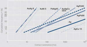
Figure 4: Distribution of cumulative frequency H of the contact resistance for solid contact rivets after 10 days exposure in a three-component test environment with 400 ppb each of H2S, SO2 and NO2 at 25°C, 75% RH; Contact force 10cN; Measuring parameters: ≤ 40 mVDC,10 mA; Probing contact: Gold rivet
