Uncategorized files
Showing below up to 250 results in range #1 to #250.
View (previous 250 | next 250) (20 | 50 | 100 | 250 | 500)
 13Dimensional Ranges.jpg 544 × 508; 43 KB
 13neuDimensional -Ranges.jpg 486 × 629; 48 KB
 14kleine Tabelle.jpg 159 × 182; 13 KB
 16Quality criteria -of standard weld -buttonsneu.jpg 1,200 × 736; 191 KB
 16Quality criteria of standard weld buttons.jpg 537 × 286; 30 KB
 Application Examples and Form of Supply for VAKURIT Materials.jpg 543 × 226; 33 KB
 Application Examples and Forms of Gold and Gold Alloys.jpg 547 × 339; 86 KB
 Application Examples and Forms of Supply for Tungsten.jpg 545 × 134; 35 KB
 Application ranges for contact materials.jpg 434 × 448; 65 KB
 Application ranges switching current and voltage.jpg 346 × 392; 51 KB
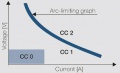
 Arc-limiting graphs.jpg 352 × 400; 41 KB
 Atomic-Properties-of-the-Most-Important-Metals.jpg 1,156 × 644; 218 KB
 Automotive relays under motor load.jpg 330 × 381; 51 KB
 Bond connection Al thick wire on clad AlSi.jpg 466 × 197; 55 KB
 Brazing Times for Different Brazing Methods.jpg 543 × 123; 17 KB
 Brush Tampon plating cell.jpg 230 × 338; 26 KB
 CdO tip on Cu carrier.jpg 315 × 199; 33 KB
 Coarse grain micro structure of Ag.jpg 319 × 283; 57 KB
 Coating composition of a printed circuit board.jpg 289 × 201; 15 KB
 Cold bonding of bimetall rivets.jpg 544 × 279; 25 KB
 Cold roll-cladding of semi-finished strips (schematic).jpg 543 × 291; 27 KB
 Commonly Used Brazing Alloys for Electrical Contacts.jpg 1,124 × 569; 120 KB
 Commonly Used Grades of Gold.jpg 545 × 319; 36 KB
 Component with hybrid housing for use in automobiles.jpg 465 × 340; 62 KB
 Computer controlled contact resistance measuring device.jpg 637 × 294; 74 KB
 Contact-resistance-of-crossed-rods.jpg 304 × 343; 48 KB
 Contact Profiles Dimensions.jpg 538 × 93; 13 KB
 Contact Profiles Dimensions and tolerances.jpg 549 × 204; 34 KB
 Contact and Switching Properties of Contact Materials Based on.jpg 544 × 270; 57 KB
 Contact and Switching Properties of Copper Tungsten.jpg 547 × 199; 36 KB
 Contact and Switching Properties of Gold and Gold Alloys.jpg 548 × 272; 48 KB
 Contact and Switching Properties of VAKURIT Materials.jpg 546 × 196; 39 KB
 Contact opening with arc formation schematic.jpg 647 × 279; 109 KB
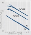
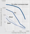 Contact resistance Rk as a function of the contact force Fk.jpg 296 × 342; 50 KB
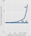 Contact resistance Rk as a function of the fretting wear cycles.jpg 294 × 341; 32 KB
 Contact resistance with exposure to out gasing from plastics.jpg 650 × 363; 78 KB
 Contact tulips with CuW welded to CuCrZr carriers.jpg 262 × 349; 26 KB
 Contilevered strip.jpg 234 × 74; 11 KB
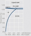 Copper corner of the copper chromium phase diagram.jpg 316 × 364; 33 KB
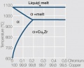 Copper corner of the copper zirconium for up to 0.5-wt zirconium.jpg 318 × 257; 30 KB
 CopyRight.png 88 × 31; 5 KB
 Different shapes of silver powders.jpg 468 × 179; 56 KB
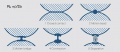
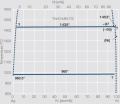
 Dimensional Ranges.jpg 545 × 114; 22 KB
 Dimensional ranges.jpg 546 × 155; 24 KB
 Dimensional ranges2.jpg 544 × 133; 22 KB
 Dimensions.jpg 494 × 145; 14 KB
 Dimensions and Tolerances.jpg 430 × 178; 28 KB
 Dimensions typical-values.jpg 494 × 80; 12 KB
 Direct press-insertion of wire segments.jpg 543 × 196; 14 KB
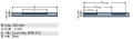
 Direction dependence of the spring bending limit.jpg 436 × 255; 47 KB
 Disc.jpg 220 × 86; 11 KB
 Dual supported strip.jpg 234 × 72; 11 KB
 Electrical-Properties-of-the-Most-Important-Metals.jpg 1,163 × 668; 217 KB
 Electrical conductivity of copper nickel alloys.jpg 292 × 283; 26 KB
 Electrical conductivity of precipitation hardened CuCr 0.6.jpg 459 × 213; 56 KB
 Electrical resistivity p of AgCu alloys.jpg 355 × 224; 24 KB
 Electrical resistivity p of PdCu alloys.jpg 265 × 254; 30 KB
 Electroless Deposition of Nickel Gold.jpg 469 × 229; 56 KB
 Electroless deposition on a printed circuit board.jpg 294 × 354; 70 KB
 Electroplated Parts.jpg 464 × 454; 82 KB
 Examples for percussion welded contact parts.jpg 541 × 358; 32 KB
 Examples of AlSi clad strips for bond connections.jpg 465 × 275; 63 KB
 Examples of Wire Welding.jpg 544 × 324; 72 KB
 Examples of assembled contact components.jpg 257 × 181; 24 KB
 Examples of brazed contact assemblies.jpg 300 × 207; 11 KB
 Examples of clad stamped parts.jpg 301 × 178; 13 KB
 Examples of pre-mounted stamped component parts.jpg 270 × 233; 16 KB
 Examples of precious metal scrap.jpg 355 × 222; 37 KB
 Examples of riveted stamped parts.jpg 269 × 280; 18 KB
 Examples of strip over molded contact components.jpg 231 × 192; 24 KB
 Examples of vacuum coated semi finished materials and parts.jpg 466 × 284; 76 KB
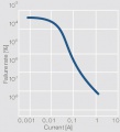 Failure probability of a contact as a function of the current.jpg 296 × 326; 23 KB
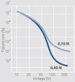 Failure probability of a contact as a function of the voitage.jpg 295 × 323; 28 KB
 Fine grain microstructure of AgNiO.jpg 316 × 286; 73 KB
 Flexible keyboard contact pattern printed with AUROMAL 170.jpg 465 × 332; 69 KB
 General Rules for Dimensioning of Contact Rivets.jpg 321 × 142; 14 KB
 Hardness of precipitation hardened CuCr 0.6.jpg 457 × 298; 68 KB
 Helical spring.jpg 216 × 137; 20 KB
 Histogram of the contact resistance Rk.jpg 374 × 494; 52 KB
 Horizontal Wire Welding Dimensions.jpg 565 × 235; 26 KB
 Horizontal profile cut-off welding (schematic).jpg 543 × 293; 28 KB
 Hot bonding of bimetal rivets.jpg 543 × 282; 25 KB
 Hot cladding of pre-materials (schematisch).jpg 542 × 188; 14 KB
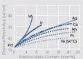
 Influence of 1-10 atomic of different.jpg 242 × 272; 19 KB
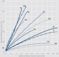
 Influence of 1 10 atom of different alloying metals.jpg 293 × 267; 33 KB
 Influence of palladium.jpg 316 × 223; 33 KB
 Influence of platinum degussa.jpg 505 × 493; 89 KB
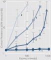 Influence of the corrosive gas concentration for four classes.jpg 329 × 382; 60 KB
 Influences on contact areas in relays.jpg 805 × 431; 80 KB
 K7-gef.png 8 × 8; 153 bytes
 K7-leer.png 9 × 10; 155 bytes
 Material transfer under DC load.jpg 648 × 286; 106 KB
 Mechanical-Properties-of-the-Most-Important-Metals.jpg 547 × 501; 92 KB
 Mechanical Properties of Gold and Gold Alloys.jpg 543 × 705; 101 KB
 Mechanical Properties of Tungsten and Molybdenum.jpg 546 × 221; 35 KB
 Mechanical properties of brass depending on the copper content.jpg 513 × 390; 89 KB
 Mechanical properties of tin bronze depending on the tin content.jpg 647 × 700; 126 KB
 Micro structure of.jpg 557 × 561; 128 KB
 Micro structure of2.jpg 547 × 536; 138 KB
 Micro structure of -Ag WC 27 C3.jpg 320 × 298; 66 KB
 Micro structure of 122.jpg 555 × 281; 66 KB
 Micro structure of 123.jpg 548 × 278; 74 KB
 Micro structure of AgCdO8812WP.jpg 655 × 262; 127 KB
 Micro structure of AgCdO9010.jpg 653 × 302; 120 KB
 Micro structure of AgCdO9010P.jpg 657 × 268; 112 KB
 Micro structure of AgCdO9010ZH.jpg 321 × 263; 64 KB
 Micro structure of AgNi9010.jpg 654 × 304; 115 KB
 Micro structure of AgNi 8020.jpg 653 × 300; 126 KB
 Micro structure of Ag C 95 5.jpg 650 × 251; 119 KB
 Micro structure of Ag C 96 4 D.jpg 651 × 308; 117 KB
 Micro structure of Ag C 97 3.jpg 659 × 254; 114 KB
 Micro structure of Ag C DF.jpg 651 × 299; 100 KB
 Micro structure of Ag Mo 35 65.jpg 320 × 295; 58 KB
 Micro structure of Ag SnO2 86 14 WPC.jpg 652 × 255; 116 KB
 Micro structure of Ag SnO2 86 14 WPX.jpg 653 × 260; 120 KB
 Micro structure of Ag SnO2 88 12 PE.jpg 654 × 264; 132 KB
 Micro structure of Ag SnO2 88 12 PW.jpg 654 × 252; 137 KB
 Micro structure of Ag SnO2 88 12 TOS F.jpg 652 × 259; 105 KB
 Micro structure of Ag SnO2 88 12 WPD.jpg 320 × 260; 52 KB
 Micro structure of Ag SnO2 88 12 WPX.jpg 318 × 260; 46 KB
 Micro structure of Ag SnO2 92 8PX.jpg 653 × 267; 124 KB
 Micro structure of Ag SnO2 92 8 PE.jpg 653 × 263; 130 KB
 Micro structure of Ag SnO2 92 8 WTOS F.jpg 656 × 252; 104 KB
 Micro structure of Ag SnO2 98 2 PX.jpg 652 × 261; 98 KB
 Micro structure of Ag WC 50 50.jpg 316 × 301; 59 KB
 Micro structure of Ag W 25 75.jpg 316 × 302; 51 KB
 Micro structure of Ag ZnO 92 8 Pw25.jpg 653 × 248; 127 KB
 Micro structure of Ag ZnO 92 8 WPW25.jpg 652 × 248; 118 KB
 Micro structure of Cu Cr 50 50 low gas.jpg 316 × 284; 66 KB
 Micro structure of Cu Cr 75 25 low gas.jpg 318 × 285; 58 KB
 Micro structure of W Cu 30Sb1.jpg 317 × 284; 58 KB
 Micro structure of W Cu 70 30 F.jpg 315 × 286; 68 KB
 Micro structure of W Cu 70 30 G.jpg 316 × 285; 53 KB
 Micro structure of W Cu 70 30 H.jpg 316 × 283; 57 KB
 Micro structure of W Cu 80 20 H.jpg 316 × 282; 57 KB
 Micro strukture of WC Ag 50 50 low gas.jpg 315 × 285; 55 KB
 Microstructure of a powder metallurgical Ag CdO material.jpg 376 × 227; 62 KB
 One side fixed contact bending spring.jpg 612 × 221; 48 KB
 Overview of the Most Widely Used Silver Grades.jpg 716 × 321; 63 KB
 Percussion welding (schematic).jpg 543 × 254; 26 KB
 Phase diagram of copper beryllium with temperature ranges.jpg 356 × 334; 48 KB
 Phase diagram of copper nickel.jpg 315 × 395; 35 KB
 Phase diagram of copper silver.jpg 326 × 403; 37 KB
 Phase diagram of copper zinc.jpg 414 × 488; 62 KB
 Phase diagram of gold-cobalt.jpg 546 × 674; 72 KB
 Phase diagram of gold-copper.jpg 383 × 449; 56 KB
 Phase diagram of gold-nickel.jpg 547 × 682; 72 KB
 Phase diagram of gold-silver.jpg 318 × 385; 30 KB
 Phase diagram of gold copper.jpg 340 × 401; 29 KB
 Phase diagram of goldplatinum.jpg 392 × 477; 54 KB
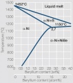 Phase diagram of nickel beryllium.jpg 306 × 345; 45 KB
 Phase diagram of palladium copper.jpg 412 × 410; 56 KB
 Phase diagram of palladium copper2.jpg 408 × 496; 70 KB
 Phase diagram of platinum iridium.jpg 463 × 473; 50 KB
 Phase diagram of platinum nickel.jpg 447 × 418; 66 KB
 Phase diagram of silver cadmium.jpg 459 × 441; 88 KB
 Phase diagram of silver copper.jpg 477 × 438; 64 KB
 Phase diagram of silver nickel.jpg 516 × 446; 57 KB
 Phase diagram of silver palladium.jpg 491 × 387; 56 KB
 Phase diagram of the Cu Sn system.jpg 290 × 513; 48 KB
 Physical Mechanical Properties as Manufacturing.jpg 900 × 800; 251 KB
 Physical Mechanical properties.pdf ; 423 KB
 Physical Properties of-Contact Materials Based.jpg 833 × 517; 116 KB
 Physical Properties of Copper Tungsten CUWODUR Contact Materials.jpg 837 × 497; 130 KB
 Physical Properties of Gold and Gold-Alloys.jpg 829 × 237; 76 KB
 Physical Properties of platinum metals.jpg 845 × 142; 48 KB
 Physical Properties of the Low Gas Materials for Vacuum Switches.jpg 957 × 293; 88 KB
 Physical and Mechanical Properties.jpg 879 × 331; 89 KB
 Porosity of an electroplated hard gold layer.jpg 292 × 338; 37 KB
 Precious metals in various forms.jpg 356 × 265; 78 KB
 Precipitation hardening of AuCo5 at.jpg 317 × 215; 22 KB
 Precipitation hardening of AuCu14Pt9Ag4.jpg 405 × 447; 55 KB
 Precipitation hardening of CuBe2 (soft) at 325C.jpg 614 × 210; 60 KB
 Precipitation hardening of CuBe2 at 325C.jpg 453 × 208; 34 KB
 Precipitation hardening of CuBe2 half hard.jpg 460 × 211; 33 KB
 Precipitation hardening of NiBe2 soft at 480C.jpg 482 × 214; 45 KB
 Principle of sputtering.jpg 466 × 255; 36 KB
 Processes for the refining of precious metal scrap.jpg 767 × 471; 98 KB
 Progressive die for stamped contact parts.jpg 460 × 371; 45 KB
 Properties production platinum metals.jpg 900 × 172; 74 KB
 Qualitaetsmerkmale und Toleranzen.jpg 544 × 200; 31 KB
 Quality criteria and tolerances.jpg 542 × 163; 17 KB
 Quality criteria dimensions and tolerances.jpg 544 × 365; 48 KB
 Ranges of fatigue strength for selected copper materials Wieland.jpg 520 × 281; 39 KB
 Relaxation behavior of selected copper based materials.jpg 469 × 294; 55 KB
 Reserved u shaped element.jpg 228 × 96; 14 KB
 Resistance brazing (schematic).jpg 544 × 246; 20 KB
 Reversed strip.jpg 240 × 65; 9 KB
 Rough flat surface.jpg 464 × 635; 118 KB
 SEM photos of silver flakes a fine grain b large flat.jpg 468 × 205; 58 KB
 Schematic describing the contact load categories.jpg 298 × 181; 19 KB
 Seam-welding process (schematic).jpg 545 × 278; 34 KB
 Shear force of an adhesive joint.jpg 212 × 215; 17 KB
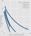
 Smallest possible bend radii for 90 bends as function.jpg 389 × 310; 47 KB
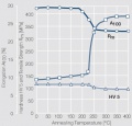
 SofteningOfCuETPafterAnnealing.png 460 × 308; 37 KB
 Softening behavior for selected copper based materials.jpg 517 × 227; 34 KB
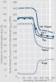
 Softening of ARGODUR 27 after annealing.jpg 339 × 342; 53 KB
 Softening of AgCdO8812WP after annealing.jpg 318 × 276; 37 KB
 Softening of AgCdO9010P after annealing.jpg 340 × 494; 70 KB
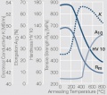
 Softening of AgCu10 after annealing.jpg 356 × 311; 53 KB
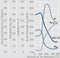
 Softening of AgCu28 after annealing.jpg 350 × 310; 51 KB
 Softening of AgCu3 after annealing.jpg 341 × 333; 53 KB
 Softening of AgCu5 after annealing.jpg 349 × 349; 56 KB
 Softening of AgNi8020 after annealing.jpg 337 × 460; 67 KB
 Softening of AgNi9010 after annealing.jpg 397 × 452; 72 KB
 Softening of AgNiO15 after annealing.jpg 315 × 295; 38 KB
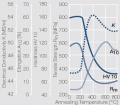
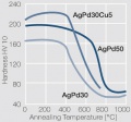 Softening of AgPd30 AgPd50 AgPd30Cu5.jpg 279 × 261; 33 KB
 Softening of AgSnO2 92 8 PE.jpg 347 × 463; 72 KB
 Softening of Ag C 96 4 D.jpg 292 × 283; 30 KB
 Softening of Ag C DF after annealing.jpg 292 × 282; 30 KB
 Softening of Ag SnO2 86 14 WPC.jpg 288 × 246; 32 KB
 Softening of Ag SnO2 88 12P after annealing.jpg 468 × 426; 63 KB
 Softening of Ag SnO2 88 12 PE after annealing.jpg 347 × 462; 71 KB
 Softening of Ag SnO2 88 12 PW4 after annealing.jpg 337 × 493; 73 KB
 Softening of Ag SnO2 88 12 TOS F after annealing.jpg 414 × 398; 54 KB
 Softening of Ag SnO2 88 12 WPC after annealing.jpg 280 × 239; 34 KB
 Softening of Ag SnO2 88 12 WPD after annealing.jpg 318 × 244; 35 KB
 Softening of Ag SnO2 88 12 WPX.jpg 284 × 245; 34 KB
 Softening of Ag SnO2 92 8 PX after annealing.jpg 480 × 437; 66 KB
 Softening of Ag SnO2 98 2 PX after annealing.jpg 480 × 443; 69 KB
 Softening of Ag ZnO 92 8 PW25.jpg 313 × 429; 64 KB
 Softening of Ag ZnO 92 8 WPW25.jpg 280 × 271; 29 KB
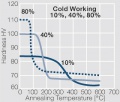
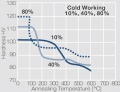
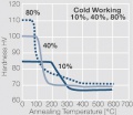
 Softening of Ag after annealing after different degrees.jpg 371 × 241; 47 KB
 Softening of AuAg20Cu10 after annealing for 0.5 hrs.jpg 368 × 270; 34 KB
 Softening of AuAg26Ni3 after annealing for 0.5-hrs.jpg 375 × 281; 36 KB
 Softening of AuNi5 after annealing for 0.5 hrs.jpg 382 × 291; 36 KB
 Softening of Au after annealing for 0.5 hrs.jpg 428 × 328; 39 KB
 Softening of CuAg2 40.jpg 523 × 247; 47 KB
 Softening of CuAg2 80.jpg 507 × 247; 48 KB
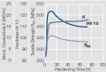
 Softening of CuCr1Zr after 1hr annealing.jpg 455 × 257; 53 KB


.jpg)


.jpg)


.jpg)


.jpg)


.jpg)


.jpg)


.jpg)
_at_325C.jpg)