File list
This special page shows all uploaded files.
| Date | Name | Thumbnail | Size | Description | Versions |
|---|---|---|---|---|---|
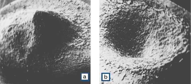
| 15:41, 1 April 2014 | Material transfer under DC load.jpg (file) |  |
106 KB | Material transfer under DC load a) Cathode; b) Anode. <br /> Material: AgNi0.15; Switching parameters: 12V<sub>DC</sub>, 3 A, 2x10<sup>6</sup> operations | 2 |
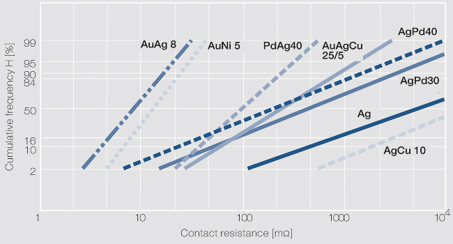
| 15:18, 1 April 2014 | Distribution of cumulative frequency H of the contact resistance for solid contact rivets.jpg (file) |  |
80 KB | Distribution of cumulative frequency H of the contact resistance for solid contact rivets after 10 days exposure in a three-component test environment with 400 ppb each of H2S, SO2 and NO2 at 25°C, 75% RH; Contact force 10cN; Measuring parameters: ≤... | 1 |
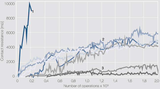
| 14:53, 1 April 2014 | Contact resistance with exposure to out gasing from plastics.jpg (file) |  |
78 KB | Contact resistance with exposure to out-gasing from plastics as a function of numbers of operations at 6 V<sub>DC</sub>,100 mA: 1 Silicon containing plastic; 2 Plastics with strongly out-gasing components; 3 Plastics with minimal out-gasing components | 1 |
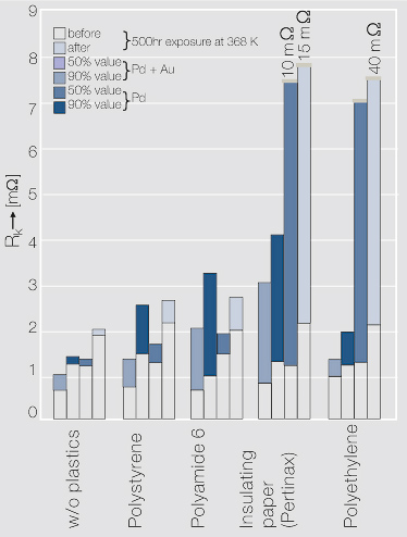
| 14:24, 1 April 2014 | Histogram of the contact resistance Rk.jpg (file) |  |
52 KB | Histogram of the contact resistance R<sub>K</ sub> of an electroplated palladium layer (3 μm) with and without hard gold flash plating (0.2 μm) after exposure with different plastic materials | 3 |
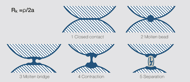
| 14:09, 1 April 2014 | Contact opening with arc formation schematic.jpg (file) |  |
109 KB | Contact opening with arc formation (schematic) | 1 |
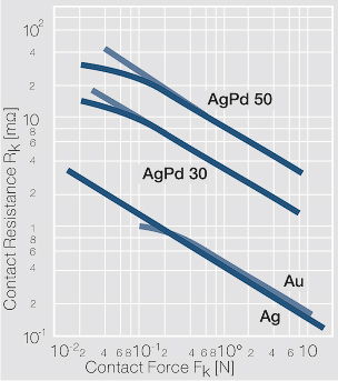
| 13:35, 1 April 2014 | Contact-resistance-of-crossed-rods.jpg (file) |  |
48 KB | Contact resistance of crossed rods as a function of the contact force for gold, silver and silver-palladium alloys | 1 |
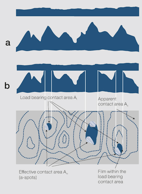
| 12:56, 1 April 2014 | Rough flat surface.jpg (file) |  |
118 KB | Rough flat surface. a) before and b) during making contact with an ideally smooth flat surface; c) Schematic of the apparent, load bearing and effective contact areas (not to scale; dashed lines are elevation lines) | 1 |
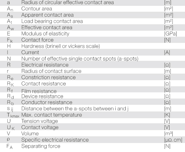
| 17:48, 26 March 2014 | Symbole used.jpg (file) |  |
109 KB | Symbole used | 1 |
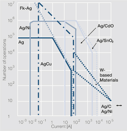
| 14:09, 26 March 2014 | Application ranges for contact materials.jpg (file) |  |
65 KB | Application ranges for contact materials in power engineering switching devices as a function of switching current and numbers of operation | 1 |
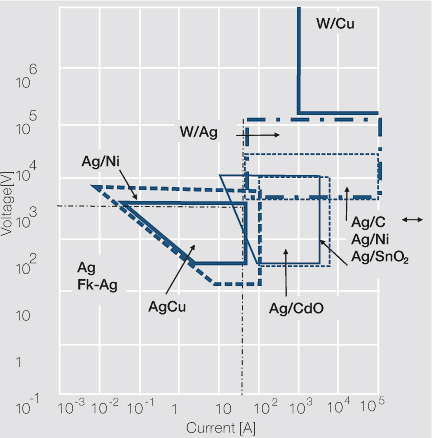
| 13:59, 26 March 2014 | Typical application ranges for contact materials.jpg (file) |  |
58 KB | Typical application ranges for contact materials in power engineering switching devices as a function of switching current and voltage | 1 |
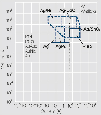
| 13:49, 26 March 2014 | Application ranges switching current and voltage.jpg (file) |  |
51 KB | Application ranges (switching current and voltage) of contact materials for information technology and transitioning into the power switching devices | 1 |
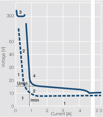
| 13:00, 26 March 2014 | Arc-limiting graphs.jpg (file) |  |
41 KB | Arc-limiting graphs (schematic) 1. Arc-less switching 2. Short instable arcs 3. Glow discharge 4. Full electrical arcs | 2 |
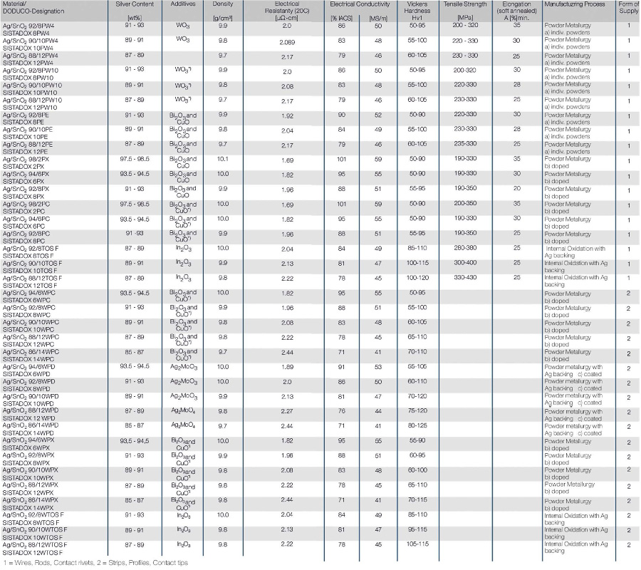
| 13:24, 18 March 2014 | Physical Mechanical Properties as Manufacturing.jpg (file) |  |
251 KB | {| |- |Description |Physical and Mechanical Properties as well as Manufacturing Processes and Forms of Supply of Extruded Silver-Tin Oxide (SISTADOX) Contact Materials Als PDF herunterladen: [[File:Physical Mechanical properties.pdf|Physical and Mechan... | 1 |
| 13:21, 18 March 2014 | Physical Mechanical properties.pdf (file) | 423 KB | Physical and Mechanical Properties as well as Manufacturing Processes and Forms of Supply of Extruded Silver-Tin Oxide (SISTADOX) Contact Materials | 1 | |
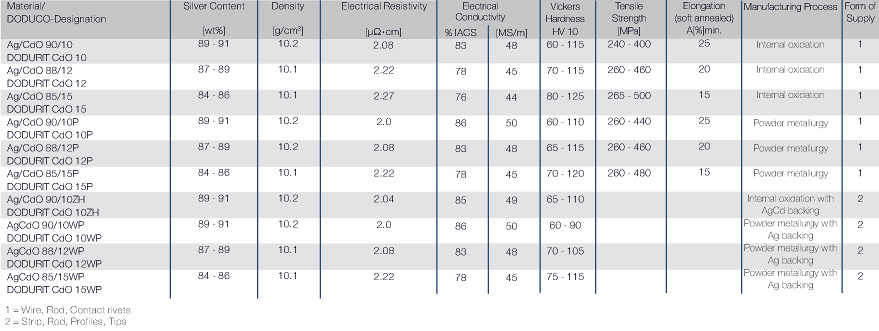
| 15:23, 17 March 2014 | Physical and Mechanical Properties.jpg (file) |  |
89 KB | Physical and Mechanical Properties as well as Manufacturing Processes and Forms of Supply of Extruded Silver Cadmium Oxide (DODURIT CdO) Contact Materials | 3 |
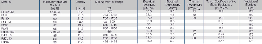
| 14:00, 12 March 2014 | Physical Properties of platinum metals.jpg (file) | 48 KB | Physical Properties of the Platinum Metals and their Alloys | 1 | |
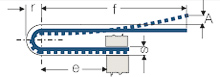
| 17:07, 11 March 2014 | Reserved u shaped element.jpg (file) |  |
14 KB | Reserved_u_shaped_element.jpg | 1 |
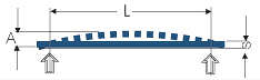
| 16:59, 11 March 2014 | Dual supported strip.jpg (file) |  |
11 KB | Dual supported strip | 2 |
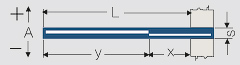
| 16:54, 11 March 2014 | Reversed strip.jpg (file) | 9 KB | Reversed_strip.jpg | 1 | |
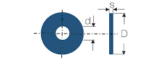
| 16:49, 11 March 2014 | Disc.jpg (file) |  |
11 KB | Disc | 2 |
| 16:38, 11 March 2014 | Helical spring.jpg (file) |  |
20 KB | Helical_spring.jpg | 2 |
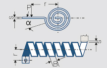
| 16:32, 11 March 2014 | Spiral.jpg (file) |  |
12 KB | Design Formulas for Thermostatic Bimetal Components | 1 |
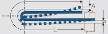
| 16:27, 11 March 2014 | U shaped element.jpg (file) |  |
14 KB | U-shaped element | 1 |
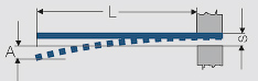
| 15:58, 11 March 2014 | Contilevered strip.jpg (file) |  |
11 KB | Contilevered strip | 1 |
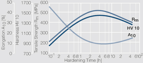
| 14:47, 4 March 2014 | Precipitation hardening of NiBe2 soft at 480C.jpg (file) |  |
45 KB | Precipitation hardening of NiBe2 (soft) at 480°C | 1 |
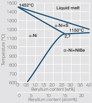
| 14:39, 4 March 2014 | Phase diagram of nickel beryllium.jpg (file) |  |
45 KB | Phase diagram of nickel-beryllium | 1 |
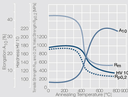
| 14:34, 4 March 2014 | Softening of NiCu30Fe after annealing for 0.5 hrs.jpg (file) |  |
53 KB | Softening of NiCu30Fe after annealing for 0.5 hrs and after 80% cold working | 1 |
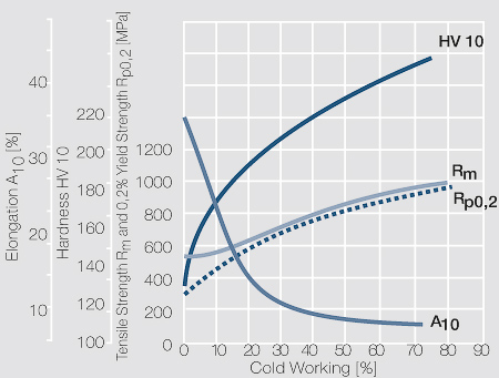
| 14:28, 4 March 2014 | Strain hardening of NiCu30Fe by cold working.jpg (file) |  |
57 KB | Strain hardening of NiCu30Fe by cold working | 1 |
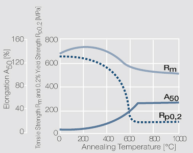
| 14:21, 4 March 2014 | Softening of technical grad nickel after annealing for 3 hrs.jpg (file) |  |
37 KB | Softening of technical grad nickel after annealing for 3 hrs after 50% cold working | 1 |
| 14:17, 4 March 2014 | Strain hardening of technical pure nickel by cold working.jpg (file) |  |
55 KB | Strain hardening of technical pure nickel by cold working | 1 |
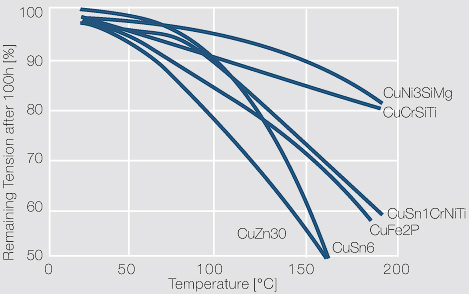
| 14:08, 4 March 2014 | Relaxation behavior of selected copper based materials.jpg (file) |  |
55 KB | Relaxation behavior of selected copper-based materials. Starting tension: 100% of spring bending limit; Stress duration: 100 hrs (Wieland) | 1 |
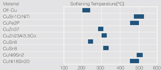
| 14:03, 4 March 2014 | Softening behavior for selected copper based materials.jpg (file) |  |
34 KB | Softening behavior for selected copper-based materials after 40% cold working (Wieland) | 1 |
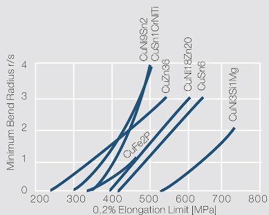
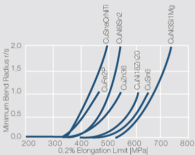
| 13:57, 4 March 2014 | Smallest possible bend radii as a functionbend line parallel to the rolling direction.jpg (file) |  |
46 KB | Smallest possible bend radii for 90° bends as a function of the 0.2% yield strength Rp0.2 – bend line parallel to the rolling direction (Wieland) | 1 |
| 13:45, 4 March 2014 | Smallest possible bend radii for 90 bends as function.jpg (file) |  |
47 KB | Smallest possible bend radii for 90° bends as a function of the 0.2% yield strength R<sub>p0.2</sub> – bend line perpendicular to the rolling direction (Wieland) | 1 |
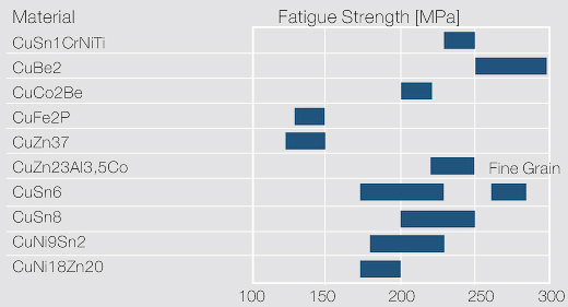
| 13:39, 4 March 2014 | Ranges of fatigue strength for selected copper materials Wieland.jpg (file) |  |
39 KB | Ranges of fatigue strength for selected copper materials (Wieland) | 1 |
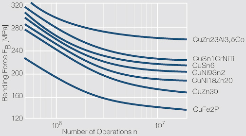
| 13:35, 4 March 2014 | Woehler curves for selected copper based materials.jpg (file) |  |
65 KB | Woehler curves for selected copper based materials. Strip samples: 0.3 mm thick, cold worked; Testfrequency; 1,500 / min (Wieland) | 1 |
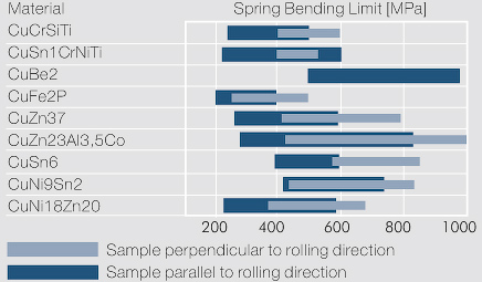
| 13:30, 4 March 2014 | Direction dependence of the spring bending limit.jpg (file) |  |
47 KB | Direction dependence of the spring bending limit of selected copper materials (Wieland) | 1 |
| 13:23, 4 March 2014 | Softening of CuCr1Zr after 1hr annealing.jpg (file) |  |
53 KB | Softening of CuCr1Zr after 1 hr annealing and after 90% cold working | 1 |
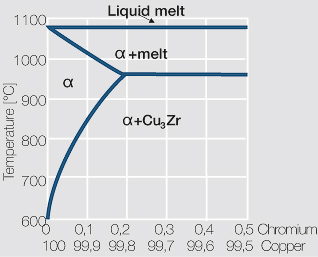
| 13:17, 4 March 2014 | Copper corner of the copper zirconium for up to 0.5-wt zirconium.jpg (file) |  |
30 KB | Copper corner of the copper- zirconium for up to 0.5 wt% zirconium | 1 |
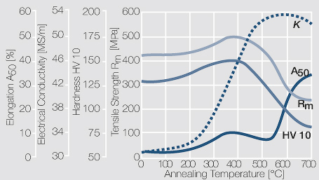
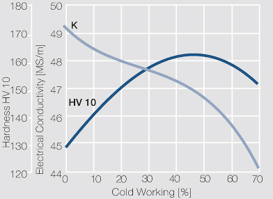
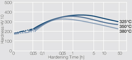
| 13:05, 4 March 2014 | Electrical conductivity and hardness of precipitation hardened CuCr 0.6.jpg (file) |  |
38 KB | Electrical conductivity and hardness of precipitation hardened CuCr 0.6 after cold working | 1 |
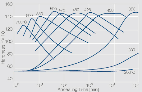
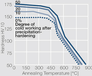
| 12:44, 4 March 2014 | Hardness of precipitation hardened CuCr 0.6.jpg (file) |  |
68 KB | Hardness of precipitation hardened CuCr 0.6 as a function of annealing conditions | 1 |
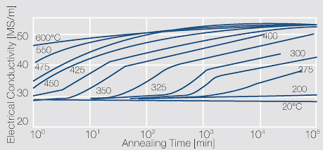
| 12:36, 4 March 2014 | Electrical conductivity of precipitation hardened CuCr 0.6.jpg (file) |  |
56 KB | Electrical conductivity of precipitation hardened CuCr 0.6 as a function of annealing conditions | 1 |
| 12:31, 4 March 2014 | Softening of precipitation hardened and subsequently cold worked CuCr1.jpg (file) |  |
38 KB | Softening of precipitation-hardened and subsequently cold worked CuCr1 after 4hrs annealing | 1 |
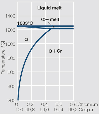
| 12:16, 4 March 2014 | Copper corner of the copper chromium phase diagram.jpg (file) |  |
33 KB | Copper corner of the copper-chromium phase diagram for up to 0.8 wt% chromium | 1 |
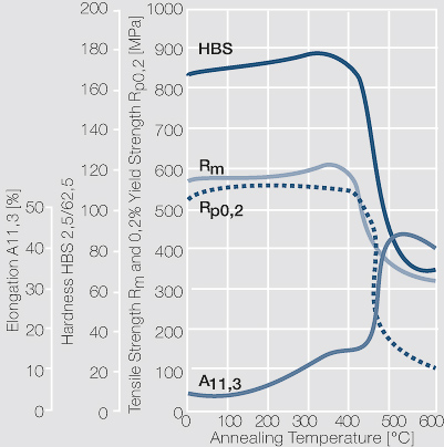
| 16:43, 3 March 2014 | Precipitation hardening of CuBe2 half hard.jpg (file) |  |
33 KB | Precipitation hardening of CuBe2 (half hard) at different annealing temperatures | 1 |
| 16:38, 3 March 2014 | Precipitation hardening of CuBe2 (soft) at 325C.jpg (file) | _at_325C.jpg) |
60 KB | Precipitation hardening of CuBe2 (soft) at 325°C | 1 |
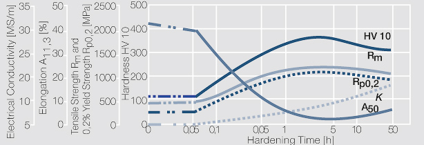
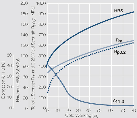
| 16:31, 3 March 2014 | Precipitation hardening of CuBe2 at 325C.jpg (file) |  |
34 KB | Precipitation hardening of CuBe2 at 325°C after different cold working | 1 |
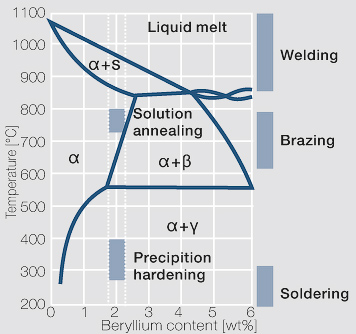
| 16:23, 3 March 2014 | Phase diagram of copper beryllium with temperature ranges.jpg (file) |  |
48 KB | Phase diagram of copper- beryllium with temperature ranges for brazing and annealing treatments | 1 |
| 16:17, 3 March 2014 | Softening of CuNi9Sn2 after annealing Wieland.jpg (file) |  |
62 KB | Softening of CuNi9Sn2 after 1 hr annealing after 60% cold working (Wieland) | 1 |
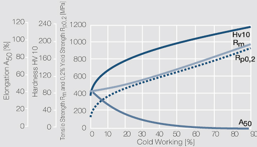
| 16:12, 3 March 2014 | Strain hardening of CuNi9Sn2 by cold working.jpg (file) |  |
67 KB | Strain hardening of CuNi9Sn2 by cold working (Wieland) | 1 |