Difference between revisions of "Applications for Bonding Technologies"
Teitscheid (talk | contribs) |
Doduco Admin (talk | contribs) (→Electroless Metal Deposition on Printed Circuit Boards) |
||
| (23 intermediate revisions by the same user not shown) | |||
| Line 1: | Line 1: | ||
| − | |||
| − | |||
== Wire Bonding== | == Wire Bonding== | ||
| − | Wire bonding is the manufacturing process for creating metallurgical bond connections between a thin wire (12.5 – 50 µm for gold fine-wires and 150 – 500 µm for aluminum thick-wires) and a suitably coated circuit carrier through friction welding. In principle this | + | Wire bonding is the manufacturing process for creating metallurgical bond connections between a thin wire (12.5 – 50 µm for gold fine-wires and 150 – 500 µm for aluminum thick-wires) and a suitably coated circuit carrier through friction welding. In principle, this method consists of pressure welding with the help of ultrasound. The metallurgical bond is mainly caused by frictional heat, created through the relative movement between the two bonding partner materials. To achieve high reliability over longer time and under difficult environmental conditions, high quality requirements regarding material and mechanical strength properties must be met by the surfaces of the bonding partners. |
| − | Multiple silicon chips are combined to a functional unit on a circuit carrier (for example PCB board, DCB substrate, thick film ceramic) which is mostly encased in a hybrid housing for environmental protection. The metallic conductors | + | Multiple silicon chips are combined to a functional unit on a circuit carrier (for example PCB board, DCB substrate, thick film ceramic) which is mostly encased in a hybrid housing for environmental protection. The metallic conductors attached inside the housing then serve as the connection to the outside. If a higher current carrying capacity is required, such as in power electronics, the Al thick wire connection is used (<xr id="fig:Bond_connection_Al_thick_wire_on_clad_AlSi"/><!--(Fig. 9.1)-->). |
<figure id="fig:Bond_connection_Al_thick_wire_on_clad_AlSi"> | <figure id="fig:Bond_connection_Al_thick_wire_on_clad_AlSi"> | ||
| − | [[File:Bond connection Al thick wire on clad AlSi.jpg|right|thumb|Bond connection: Al thick-wire on clad AlSi; (a) Macro photograph, b) micro structure with ruptured wire]] | + | [[File:Bond connection Al thick wire on clad AlSi.jpg|right|thumb|Figure 1: Bond connection: Al thick-wire on clad AlSi; (a) Macro photograph, b) micro structure with ruptured wire]] |
</figure> | </figure> | ||
| − | == AlSi Clad Strip for Bond Connections== | + | ==AlSi Clad Strip for Bond Connections== |
| − | Besides electroplated or chemically deposited gold coatings AlSi clad semi- finished materials are used for layered systems on circuit carriers and in hybrid housings (or for lead frames). These strip materials are manufactured by cold roll cladding of an AlSi1 alloy material onto Cu or Cu alloy strip (see chapter [[Manufacturing_of_Semi-Finished_Materials|Manufacturing of Semi-Finished Materials]]). | + | Besides electroplated or chemically deposited gold coatings, AlSi clad semi- finished materials are used for layered systems on circuit carriers and in hybrid housings (or for lead frames). These strip materials are manufactured by cold roll cladding of an AlSi1 alloy material onto Cu or Cu alloy strip (<xr id="fig:Examples of AlSi clad strips for bond connections"/>) (see chapter [[Manufacturing_of_Semi-Finished_Materials|Manufacturing of Semi-Finished Materials]]). |
| − | To achieve a strong metallurgical bond between these two components a suitable surface preparation of the carrier strip and a high degree of deformation are required, followed by diffusion annealing of the clad strip. | + | To achieve a strong metallurgical bond between these two components, a suitable surface preparation of the carrier strip and a high degree of deformation are required, followed by diffusion annealing of the clad strip. |
| − | Depending on the requirements of the assembly technology for the final product, i.e. using connectors or soldering attachment, the clad strips are coated in the terminal area with a suitable surface layer with either an electroplated hard gold (AuCo0.3) layer or selectively by electroplating or hot dip tinning with pure tin or a tin alloy. To ensure the best bond properties during the coating process the AlSi surface is protected against corrosion by masking during this processing step. | + | Depending on the requirements of the assembly technology for the final product, i.e. using connectors or soldering attachment, the clad strips are coated in the terminal area with a suitable surface layer with either an electroplated hard gold (AuCo0.3) layer or selectively by electroplating or hot dip tinning with pure tin or a tin alloy. To ensure the best bond properties during the coating process, the AlSi surface is protected against corrosion by masking during this processing step. |
| − | + | '''Examples of AlSi clad strips for bond connections''' | |
| − | + | <figure id="fig:Examples of AlSi clad strips for bond connections"> | |
| − | [[File:Examples of AlSi clad strips for bond connections.jpg|left|Examples of AlSi clad strips for bond connections]] | + | [[File:Examples of AlSi clad strips for bond connections.jpg|left|Figure 2: Examples of AlSi clad strips for bond connections]] |
| + | </figure> | ||
<div class="clear"></div> | <div class="clear"></div> | ||
| − | + | '''Materials''' | |
{| class="twocolortable" style="text-align: left; font-size: 12px;width:35%" | {| class="twocolortable" style="text-align: left; font-size: 12px;width:35%" | ||
| Line 32: | Line 31: | ||
|} | |} | ||
| − | + | '''Dimensions (typical values)''' | |
[[File:Dimensions typical-values.jpg|left|Dimensions (typical values)]] | [[File:Dimensions typical-values.jpg|left|Dimensions (typical values)]] | ||
<div class="clear"></div> | <div class="clear"></div> | ||
| − | + | '''Quality Criteria and Tolerances''' | |
Mechanical strength and dimensional tolerances for AlSi clad strips mostly follow the standards EN 1652, EN 1654, and EN 1758 for Cu and Cu alloys. Depending on the end application the following parameters for the coating layer are tested for and documented during manufacturing: | Mechanical strength and dimensional tolerances for AlSi clad strips mostly follow the standards EN 1652, EN 1654, and EN 1758 for Cu and Cu alloys. Depending on the end application the following parameters for the coating layer are tested for and documented during manufacturing: | ||
| Line 46: | Line 45: | ||
*Solderability | *Solderability | ||
| − | == Electroless Metal Deposition on Printed Circuit Boards== | + | ==Electroless Metal Deposition on Printed Circuit Boards== |
| − | Printed circuit boards are also used as circuit carriers. Since many of the conductive structures are not electrically connected | + | Printed circuit boards are also used as circuit carriers. Since many of the conductive structures on the PCB are not electrically connected, the final surface coatings are produced using an electroless process (<xr id="fig:Electroless deposition on a printed circuit board"/>) (Chapter [[Electroless_Plating|Electroless Plating]]). Besides bonding to Nickel/Gold surfaces, soldering is the most widely used process to create conductive connections. This can also be performed on electroless deposited tin surface coatings. |
| − | |||
<figure id="fig:Electroless deposition on a printed circuit board"> | <figure id="fig:Electroless deposition on a printed circuit board"> | ||
| − | [[File:Electroless deposition on a printed circuit board.jpg|right|thumb|Electroless deposition on a printed circuit board]] | + | [[File:Electroless deposition on a printed circuit board.jpg|right|thumb|Figure 3: Electroless deposition on a printed circuit board]] |
</figure> | </figure> | ||
Latest revision as of 13:42, 10 January 2023
Contents
Wire Bonding
Wire bonding is the manufacturing process for creating metallurgical bond connections between a thin wire (12.5 – 50 µm for gold fine-wires and 150 – 500 µm for aluminum thick-wires) and a suitably coated circuit carrier through friction welding. In principle, this method consists of pressure welding with the help of ultrasound. The metallurgical bond is mainly caused by frictional heat, created through the relative movement between the two bonding partner materials. To achieve high reliability over longer time and under difficult environmental conditions, high quality requirements regarding material and mechanical strength properties must be met by the surfaces of the bonding partners.
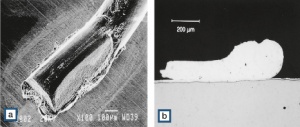
Multiple silicon chips are combined to a functional unit on a circuit carrier (for example PCB board, DCB substrate, thick film ceramic) which is mostly encased in a hybrid housing for environmental protection. The metallic conductors attached inside the housing then serve as the connection to the outside. If a higher current carrying capacity is required, such as in power electronics, the Al thick wire connection is used (Figure 1).
AlSi Clad Strip for Bond Connections
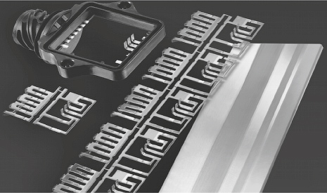
Besides electroplated or chemically deposited gold coatings, AlSi clad semi- finished materials are used for layered systems on circuit carriers and in hybrid housings (or for lead frames). These strip materials are manufactured by cold roll cladding of an AlSi1 alloy material onto Cu or Cu alloy strip (Figure 2) (see chapter Manufacturing of Semi-Finished Materials).
To achieve a strong metallurgical bond between these two components, a suitable surface preparation of the carrier strip and a high degree of deformation are required, followed by diffusion annealing of the clad strip.
Depending on the requirements of the assembly technology for the final product, i.e. using connectors or soldering attachment, the clad strips are coated in the terminal area with a suitable surface layer with either an electroplated hard gold (AuCo0.3) layer or selectively by electroplating or hot dip tinning with pure tin or a tin alloy. To ensure the best bond properties during the coating process, the AlSi surface is protected against corrosion by masking during this processing step.
Examples of AlSi clad strips for bond connections
Materials
| Inlay cladding | AISi 1 |
| Substrate materials | Cu, CuFe2P, CuSn6 others |
Dimensions (typical values)
Quality Criteria and Tolerances
Mechanical strength and dimensional tolerances for AlSi clad strips mostly follow the standards EN 1652, EN 1654, and EN 1758 for Cu and Cu alloys. Depending on the end application the following parameters for the coating layer are tested for and documented during manufacturing:
- Layer thickness
- Adhesion strength
- Bond properties
- Solderability
Electroless Metal Deposition on Printed Circuit Boards
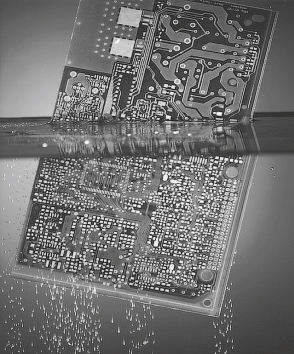
Printed circuit boards are also used as circuit carriers. Since many of the conductive structures on the PCB are not electrically connected, the final surface coatings are produced using an electroless process (Figure 3) (Chapter Electroless Plating). Besides bonding to Nickel/Gold surfaces, soldering is the most widely used process to create conductive connections. This can also be performed on electroless deposited tin surface coatings.
References
Kaspar, F.: Drahtbonden zur Kontaktierung auf elektronischen Baugruppen. VDE-Fachbericht 55 (1999) 97-103
Freudenberger, R.; Ganz, J.; Kaspar, F.; Marka, E.: REDOR reduktives Goldbad. Metalloberfläche 49 (1995) H.11, 859-862
Falk, J.; Lutz, K.; Berchthold, L.; Ritz, K.: Oberflächen zum Drahtbonden. DVS-Bericht 141: Verbindungstechnik in der Elektronik. (1992) 178
Sheaffer, M.: Drahtbonden für neue Bauelementeumhüllungen. DVS-Bericht 141: Verbindungstechnik in der Elektronik. (1992) 48 DVS-Merkblatt 2810: Drahtbonden, Düsseldorf: DVS-Verlag 1992
Ganz, J.; Kaspar, F.: AlSi-plattierte Bänder für Bondverbindungen mit hoher Zuverlässigkeit in der Gehäusetechnik. PLUS 11 (2005) 2057 -2058


