Difference between revisions of "File:Histogram of the contact resistance Rk.jpg"
From Electrical Contacts
(Histogram of the contact resistance R<sub>K</sub> of an electroplated palladium layer (3 μm) with and without hard gold flash plating (0.2 μm) after exposure with different plastic materials) |
(No difference)
|
Revision as of 14:20, 1 April 2014
Summary
Histogram of the contact resistance RK of an electroplated palladium layer (3 μm) with and without hard gold flash plating (0.2 μm) after exposure with different plastic materials
Licensing
| Dieses Werk ist lizenziert unter einer Creative Commons Namensnennung-Nicht kommerziell 4.0 International Lizenz |
File history
Click on a date/time to view the file as it appeared at that time.
| Date/Time | Thumbnail | Dimensions | User | Comment | |
|---|---|---|---|---|---|
| current | 14:24, 1 April 2014 |  | 374 × 494 (52 KB) | Doduco Redaktion (talk | contribs) | Histogram of the contact resistance R<sub>K</ sub> of an electroplated palladium layer (3 μm) with and without hard gold flash plating (0.2 μm) after exposure with different plastic materials |
| 14:23, 1 April 2014 |  | 374 × 494 (52 KB) | Doduco Redaktion (talk | contribs) | Histogram of the contact resistance R<sub>K< /sub> of an electroplated palladium layer (3 μm) with and without hard gold flash plating (0.2 μm) after exposure with different plastic materials | |
| 14:20, 1 April 2014 | 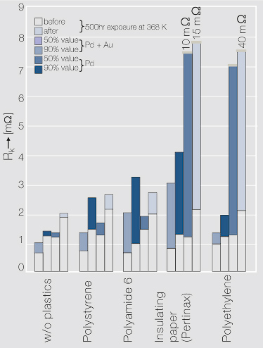 | 374 × 494 (52 KB) | Doduco Redaktion (talk | contribs) | Histogram of the contact resistance R<sub>K</sub> of an electroplated palladium layer (3 μm) with and without hard gold flash plating (0.2 μm) after exposure with different plastic materials |
- You cannot overwrite this file.
File usage
The following 2 pages link to this file: