Manufacturing of Semi-Finished Materials
Semi-finished contact pre-materials can be manufactured from solid precious metals, precious metal alloys or precious metal containing composite materials. They are made in wire, strip and profile form by known processing technologies such as extrusion and subsequent annealing and drawing or roll-forming. They are supplied following the manufacturer's internal standards usually related to DIN EN specifications for copper based materials. The most important materials are two – or multiple material layered semi-finished materials with the contact material bonded in its solid phase to non-precious carriers by cladding, brazing or welding. The contact material can also be deposited on the carrier from the liquid or vapor phase.
Contents
Clad Semi-Finished Pre-Materials (Contact-Bimetals)
Clad materials consist of two or more layers of different materials, the contact material and the carrier, which are firmly bonded to each other. Depending on the electrical requirements the contact material is mainly an alloy of gold, palladium or silver based, while the carrier material are mainly copper alloys. To bond these materials, various technologies are utilized, the two most important ones being described in more detail below.
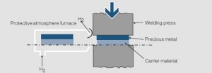
During hot cladding, the classic process, the materials to be clad are assembled into a cladding package in block or plate form, heated to about 800°C and clad (or "welded") together under high pressure (Figure 1). At the interface between the two materials, a non-separable bond is formed by either diffusion of the reaction partners or in liquid phase by forming a AgCu eutectic alloy when an additional brazing alloy foil is placed between the two materials. Further processing is done by rolling with required annealing steps between subsequent thickness reductions. The disadvantage of this process is the usually limited short length of final material strips.
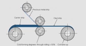
In the Cold Roll-Cladding process, the bond between the contact and carrier material is achieved by cold deformation of > 50% in one rolling pass (Figure 2). The high plastic deformation causes cold welding in the boundary layer between the two materials. To increase the quality and strength of the bond, a subsequent diffusion annealing is performed in most cases. This process is most suitable for clad semi-finished strips with thin contact material layers (≥ 2 μm) and large strip length (> 100 m).
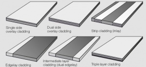
- Typical configurations of clad contact strips (Figure 3)
- Contact materials
Ag, Ag-alloys., Ag/Ni, in special cases also Ag/SnO2 and Ag/ZnO
- Carrier materials: Cu, CuSn, CuNiZn, CuNiSn, CuFe, CuBe et al.
- Dimensions (Figure 4)
When specifying the contact material layer thickness it is recommended to use the minimum required thickness.
- Quality criteria and tolerances
Strength properties and dimensional tolerances of clad contact bi-metals are derived from the standards DIN EN 1652 and DIN EN 1654 for Cu alloys. When specifying the width of the contact material layer, it is recommended to use the minimum required value. All dimensions should be specified originating from one strip edge.
Brazed Semi-Finished Contact Materials (Toplay–Profiles)
The toplay process starts with a flat or profile – shaped contact material strip which is fed together with the wider non-precious carrier material and in most cases an intermediate thin foil of brazing alloy into a induction brazing machine (Figure 5). An evenly distributed and reliable braze joint can be achieved this way between contact and carrier materials. The combined material strip is rather soft after the brazing process and re-hardened during a subsequent profile rolling step. In this way different shapes and configurations can easily be achieved.
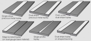
- Typical configurations of toplay contact profiles (Figure 6)
- Contact materials
Ag, AgNi 0,15, AgCu, AgCuNi (ARGODUR 27), Ag/Ni, Ag/SnO2 and Ag/ZnO
- Carrier materials: Cu, CuZn, CuSn et al.
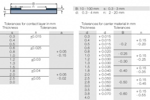
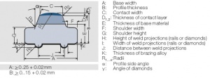
- Quality criteria, dimensions and tolerances (Figure 7)
Strength properties and dimensional tolerances of toplay profiles are derived from the standards DIN EN 1652 and DIN EN 1654 for Cu alloys.
Contact Profiles (Contact Weld Tapes)
Contact profiles span a broad range of dimensions. Width and thickness are typically between 0.8 – 8.0 mm and 0.2 – 3.0 mm resp. Special configurations, often defined as miniature-profiles or even micro–profiles can have a width < 2.0 mm.
Miniature–profiles are mostly composed of a contact-bimetal material with the contact material being a precious metal alloy or composite material clad, welded or coated by electroplating or vacuum-deposition (sputtered) onto a weldable base material. Since these profiles are attached to carrier strip materials, usually by segment– or seam– welding to the base materials, materials with good welding properties such as nickel, copper-nickel, copper-tin, as well as copper-nickel-zinc alloys are used. The bottom surface of the profiles usually has formed weld rails or similar patterns to ensure a solid continuous metallurgical weld joint between the profile and the contact carrier.
Contact profiles in larger sizes are often used for switching devices in the low voltage technology. For these, the contact layer mostly consists of arc erosion resistant materials such as silver–nickel, silver–metal oxides or the weld resistant silver– graphite. The brazable or weldable underside of the metal oxide or silver–graphite materials is usually pure silver with also quite often a thin layer of a phosphorous containing brazing alloy applied to aid the welding process.
- Typical configurations of multi-layer contact profiles (Figure 8)
- Contact materials
Au-Alloys, Pd-Alloys, Ag-Alloys, Ag/Ni, Ag/SnO2, Ag/ZnO
- Carrier materials
(weldable substrate material for multi-layer materials) Cu, Ni, CuNiFe, CuNiZn, CuSn, CuNiSn, NiCuFe
- Brazing alloy
L-Ag15P
- Quality criteria
Beause of the variety of configurations of contact profiles, usually the quality issues are separately agreed upon between the manufacturer and the user.
- Dimensions and tolerances (Figure 9)
The thickness of the Au top-layer, which is sputtered for example, is between 0.2 and 5 μm, depending on the requirements. Tolerance of thickness is about ± 10%.
