File list
This special page shows all uploaded files.
| Date | Name | Thumbnail | Size | User | Description | Versions |
|---|---|---|---|---|---|---|
| 14:09, 10 December 2013 | Dimensional ranges2.jpg (file) | 22 KB | Doduco Redaktion | Dimensional ranges | 1 | |
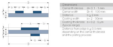
| 15:36, 20 January 2014 | Dimensions.jpg (file) |  |
14 KB | Doduco Redaktion | Dimensions | 1 |
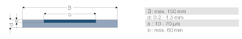
| 13:07, 10 April 2014 | Dimensions and Tolerances.jpg (file) |  |
28 KB | Doduco Redaktion | Dimensions and Tolerances | 1 |
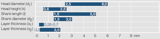
| 15:50, 15 April 2014 | Dimensions typical-values.jpg (file) | 12 KB | Doduco Redaktion | Dimensions (typical values) | 1 | |
| 12:17, 22 January 2014 | Direct press-insertion of wire segments.jpg (file) |  |
14 KB | Doduco Redaktion | Direct press-insertion of wire segments | 1 |
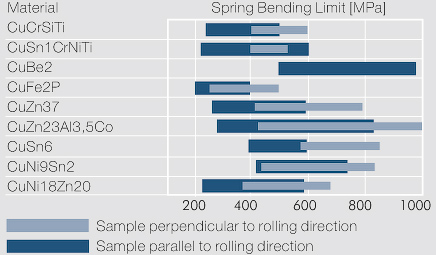
| 13:30, 4 March 2014 | Direction dependence of the spring bending limit.jpg (file) |  |
47 KB | Doduco Redaktion | Direction dependence of the spring bending limit of selected copper materials (Wieland) | 1 |
| 16:49, 11 March 2014 | Disc.jpg (file) |  |
11 KB | Doduco Redaktion | Disc | 2 |
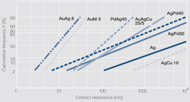
| 15:18, 1 April 2014 | Distribution of cumulative frequency H of the contact resistance for solid contact rivets.jpg (file) |  |
80 KB | Doduco Redaktion | Distribution of cumulative frequency H of the contact resistance for solid contact rivets after 10 days exposure in a three-component test environment with 400 ppb each of H2S, SO2 and NO2 at 25°C, 75% RH; Contact force 10cN; Measuring parameters: ≤... | 1 |
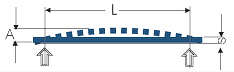
| 16:59, 11 March 2014 | Dual supported strip.jpg (file) |  |
11 KB | Doduco Redaktion | Dual supported strip | 2 |
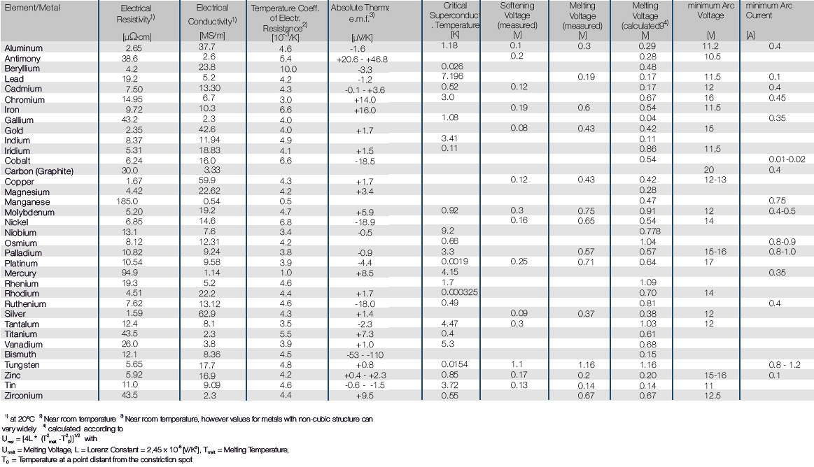
| 15:02, 12 December 2013 | Electrical-Properties-of-the-Most-Important-Metals.jpg (file) |  |
217 KB | Doduco Redaktion | Electrical Properties of the Most Important Metals | 1 |
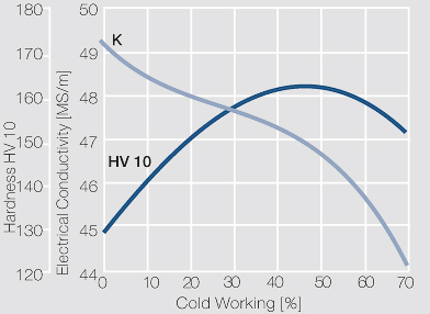
| 13:05, 4 March 2014 | Electrical conductivity and hardness of precipitation hardened CuCr 0.6.jpg (file) |  |
38 KB | Doduco Redaktion | Electrical conductivity and hardness of precipitation hardened CuCr 0.6 after cold working | 1 |
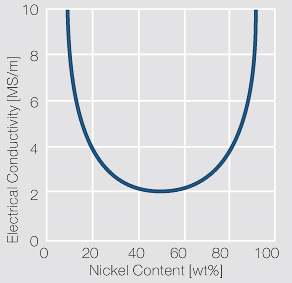
| 18:46, 20 February 2014 | Electrical conductivity of copper nickel alloys.jpg (file) |  |
26 KB | Doduco Redaktion | Electrical conductivity of copper-nickel alloys as a function of nickel content | 1 |
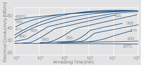
| 12:36, 4 March 2014 | Electrical conductivity of precipitation hardened CuCr 0.6.jpg (file) |  |
56 KB | Doduco Redaktion | Electrical conductivity of precipitation hardened CuCr 0.6 as a function of annealing conditions | 1 |
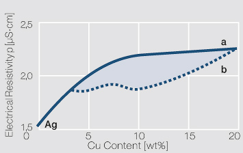
| 18:00, 11 February 2014 | Electrical resistivity p of AgCu alloys.jpg (file) |  |
24 KB | Doduco Redaktion | Electrical resistivity p of AgCu alloys with 0-20 weight% Cu in the soft annealed and tempered stage a) Annealed and quenched b) Tempered at 280°C | 1 |
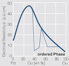
| 19:07, 7 February 2014 | Electrical resistivity p of PdCu alloys.jpg (file) |  |
30 KB | Doduco Redaktion | Electrical resistivity p of PdCu alloys with and without an annealing step for forming an ordered phase | 1 |
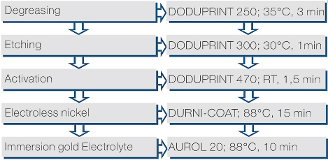
| 13:45, 10 April 2014 | Electroless Deposition of Nickel Gold.jpg (file) |  |
56 KB | Doduco Redaktion | Electroless Deposition of Nickel/Gold | 1 |
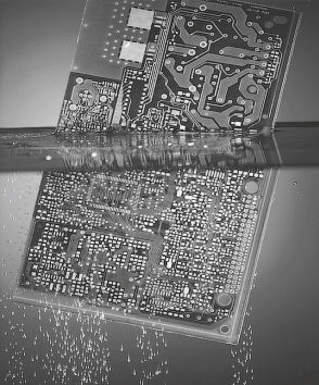
| 16:22, 15 April 2014 | Electroless deposition on a printed circuit board.jpg (file) |  |
70 KB | Doduco Redaktion | Electroless deposition on a printed circuit board | 1 |
| 16:52, 7 April 2014 | Electroplated Parts.jpg (file) |  |
82 KB | Doduco Redaktion | Electroplated Parts | 1 |
| 15:24, 22 January 2014 | Examples for percussion welded contact parts.jpg (file) |  |
32 KB | Doduco Redaktion | Examples for percussion welded contact parts | 1 |
| 15:41, 15 April 2014 | Examples of AlSi clad strips for bond connections.jpg (file) |  |
63 KB | Doduco Redaktion | Examples of AlSi clad strips for bond connections | 1 |
| 14:59, 22 January 2014 | Examples of Wire Welding.jpg (file) |  |
72 KB | Doduco Redaktion | Examples of Wire Welding | 1 |
| 17:01, 15 April 2014 | Examples of assembled contact components.jpg (file) |  |
24 KB | Doduco Redaktion | Examples of assembled contact components | 1 |
| 12:43, 22 January 2014 | Examples of brazed contact assemblies.jpg (file) |  |
11 KB | Doduco Redaktion | Examples of brazed contact assemblies | 1 |
| 16:40, 22 January 2014 | Examples of clad stamped parts.jpg (file) |  |
13 KB | Doduco Redaktion | Examples of clad stamped parts | 1 |
| 16:52, 22 January 2014 | Examples of pre-mounted stamped component parts.jpg (file) |  |
16 KB | Doduco Redaktion | Examples of pre-mounted stamped component parts | 1 |
| 11:47, 16 April 2014 | Examples of precious metal scrap.jpg (file) |  |
37 KB | Doduco Redaktion | Examples of precious metal scrap | 1 |
| 16:45, 22 January 2014 | Examples of riveted stamped parts.jpg (file) |  |
18 KB | Doduco Redaktion | Examples of riveted stamped parts | 1 |
| 16:55, 15 April 2014 | Examples of strip over molded contact components.jpg (file) |  |
24 KB | Doduco Redaktion | Examples of strip over-molded contact components | 1 |
| 14:35, 10 April 2014 | Examples of vacuum coated semi finished materials and parts.jpg (file) |  |
76 KB | Doduco Redaktion | Examples of vacuum coated semi-finished materials and parts | 1 |
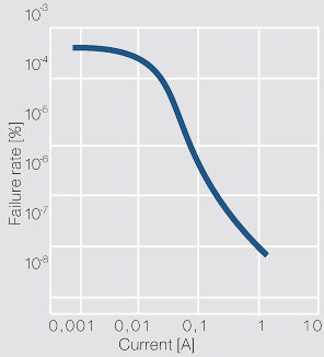
| 15:56, 7 April 2014 | Failure probability of a contact as a function of the current.jpg (file) |  |
23 KB | Doduco Redaktion | Failure probability of a contact as a function of the current (according to Kirchdorfer); Ag/Ni10; F<sub>k</sub> = 0.45 N; U = 24 V | 1 |
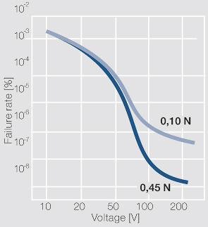
| 15:47, 7 April 2014 | Failure probability of a contact as a function of the voitage.jpg (file) |  |
28 KB | Doduco Redaktion | Failure probability of a contact as a function of the voltage (according to Kirchdorfer); Ag/Ni10; 10 mA | 1 |
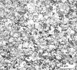
| 18:32, 11 February 2014 | Fine grain microstructure of AgNiO.jpg (file) |  |
73 KB | Doduco Redaktion | Fine grain microstructure of AgNi0.15 after 80% cold working and 1 hr annealing at 600°C | 1 |
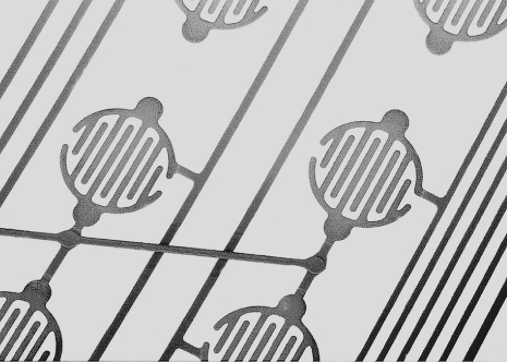
| 14:27, 15 April 2014 | Flexible keyboard contact pattern printed with AUROMAL 170.jpg (file) |  |
69 KB | Doduco Redaktion | Flexible keyboard contact pattern printed with AUROMAL 170 | 1 |
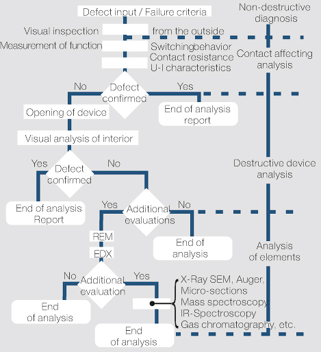
| 11:32, 23 April 2014 | Flow diagram for evaluation of failure cause in switching devices for communications technology.jpg (file) |  |
86 KB | Doduco Redaktion | Flow diagram for evaluation of failure cause in switching devices for communications technology | 1 |
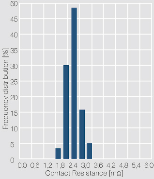
| 16:09, 16 April 2014 | Frequency distribution of the contact resistance of a clean contact surface.jpg (file) |  |
37 KB | Doduco Redaktion | Frequency distribution of the contact resistance of a clean contact surface (Ag rivet with electroplated hard gold layer; test parameters: 10 mV, 10 mA, 10 cN) | 1 |
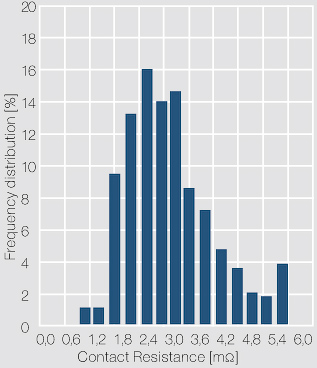
| 16:19, 16 April 2014 | Frequency distribution of the contact resistance of a contaminated contact surface.jpg (file) |  |
42 KB | Doduco Redaktion | Frequency distribution of the contact resistance of a contaminated contact surface (Ag rivet with electroplated hard gold layer; test parameters: 10 mV, 10 mA, 10 cN) | 1 |
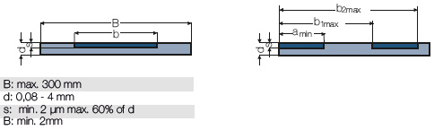
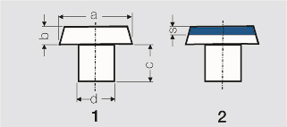
| 11:24, 2 April 2014 | General Rules for Dimensioning of Contact Rivets.jpg (file) |  |
14 KB | Doduco Redaktion | General Rules for Dimensioning of Contact Rivets | 1 |
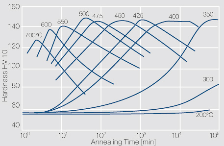
| 12:44, 4 March 2014 | Hardness of precipitation hardened CuCr 0.6.jpg (file) |  |
68 KB | Doduco Redaktion | Hardness of precipitation hardened CuCr 0.6 as a function of annealing conditions | 1 |
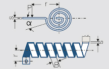
| 16:38, 11 March 2014 | Helical spring.jpg (file) |  |
20 KB | Doduco Redaktion | Helical_spring.jpg | 2 |
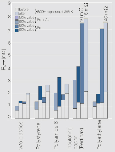
| 14:24, 1 April 2014 | Histogram of the contact resistance Rk.jpg (file) |  |
52 KB | Doduco Redaktion | Histogram of the contact resistance R<sub>K</ sub> of an electroplated palladium layer (3 μm) with and without hard gold flash plating (0.2 μm) after exposure with different plastic materials | 3 |
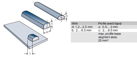
| 15:20, 22 January 2014 | Horizontal Wire Welding Dimensions.jpg (file) |  |
26 KB | Doduco Redaktion | Dimensions | 1 |
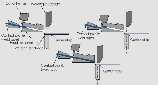
| 13:49, 22 January 2014 | Horizontal profile cut-off welding (schematic).jpg (file) | .jpg) |
28 KB | Doduco Redaktion | Horizontal profile cut-off welding (schematic) | 1 |
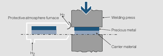
| 13:05, 10 December 2013 | Hot bonding of bimetal rivets.jpg (file) |  |
25 KB | Doduco Redaktion | Hot bonding of bimetal rivets | 1 |
| 15:06, 20 January 2014 | Hot cladding of pre-materials (schematisch).jpg (file) | .jpg) |
14 KB | Doduco Redaktion | Hot cladding of pre-materials (schematisch) | 1 |
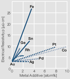
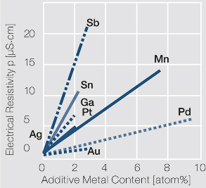
| 15:22, 16 December 2013 | Influence of 1-10 atomic of different.jpg (file) |  |
19 KB | Doduco Redaktion | Influence of 1-10 atomic% of different alloying metals on the electrical resistivity of gold (according to J. O. Linde) | 1 |
| 17:46, 11 February 2014 | Influence of 1 10 atom of different alloying metals.jpg (file) |  |
33 KB | Doduco Redaktion | Influence of 1-10 atom% of different alloying metals on the electrical resistivity of silver | 1 |
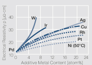
| 15:24, 7 February 2014 | Influence of palladium.jpg (file) |  |
33 KB | Doduco Redaktion | Influence of 1-22 atom% of different additive metals on the electrical resistivity p of palladium | 1 |
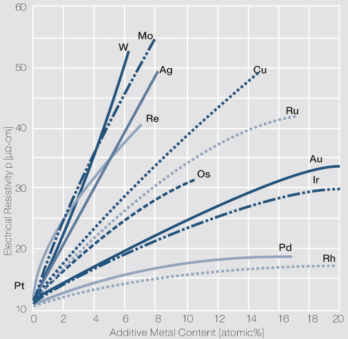
| 15:16, 7 February 2014 | Influence of platinum degussa.jpg (file) |  |
89 KB | Doduco Redaktion | Influence of 1- 20 atom% of different additive metals on the electrical resistivity p of platinum (Degussa) | 1 |
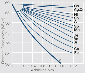
| 15:28, 20 February 2014 | Influence of small additions on the electrical conductivity of copper.jpg (file) |  |
65 KB | Doduco Redaktion | Influence of small additions on the electrical conductivity of copper | 1 |
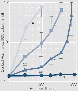
| 11:20, 24 April 2014 | Influence of the corrosive gas concentration for four classes.jpg (file) |  |
60 KB | Doduco Redaktion | Influence of the corrosive gas concentration for four classes (I–IV) on the contact resistance of a porous gold layer as a function of the exposure time (Battelle) | 1 |